Method for measuring drift amount of buried graph after epitaxial growth

A technology of pattern drift and epitaxial growth, applied in measurement devices, instruments, optical devices, etc., can solve problems such as measurement accuracy of only 0.1 μm, inability to measure measurement, and complicated operation, and achieves reduction of human bias, simple method, and measurement. simple steps

Inactive Publication Date: 2012-11-21
NO 24 RES INST OF CETC
View PDF5 Cites 4 Cited by
  • Summary
  • Abstract
  • Description
  • Claims
  • Application Information

AI Technical Summary

Problems solved by technology

Disadvantages of this method: 1) If the angle grinding and dyeing are not done well, it will cause inability to measure or inaccurate measurement, and rework and reprocessing are required; 2) This method has cumbersome steps, complicated operation, and low precision
At present, the measurement deviation of the conventional grinding angle dyeing method is usually at the level of 1 μm, and its measurement accuracy is only at the level of 0.1 μm

Method used


Image

  • Method for measuring drift amount of buried graph after epitaxial growth
  • Method for measuring drift amount of buried graph after epitaxial growth
  • Method for measuring drift amount of buried graph after epitaxial growth

Examples


Embodiment Construction

[0031] The present invention will be described in further detail below in conjunction with accompanying drawings and examples.

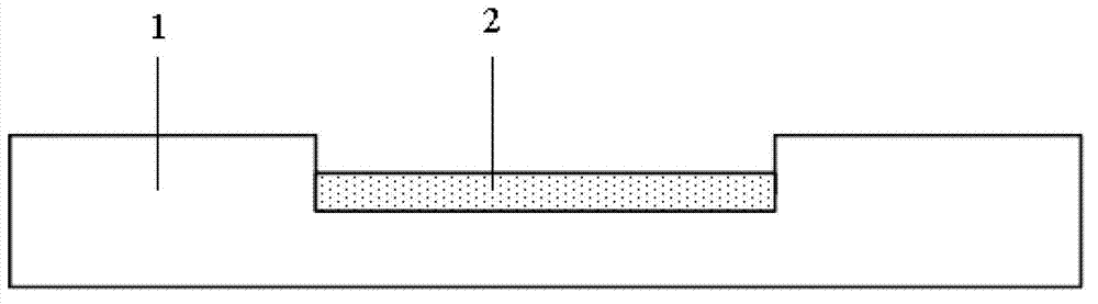
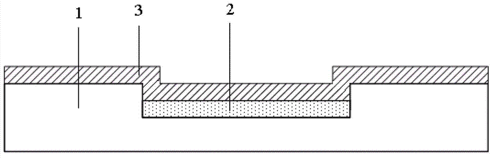
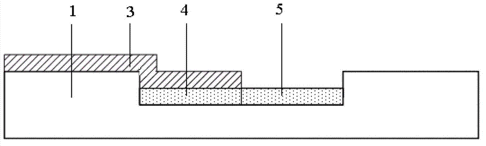
[0032] The method for measuring the drift of buried layer pattern after epitaxial growth of the present invention is to utilize the feature that selective epitaxial growth technology can carry out epitaxial growth in a specific area of ​​silicon substrate material, and other areas do not carry out epitaxial growth, to realize the same buried layer pattern. Epitaxial growth does not occur in protected areas and epitaxial growth occurs in unprotected areas. By measuring the relative position data of the protected area and the unprotected area, the drift data of the buried layer pattern after epitaxy is obtained. Concrete method of the present invention is as follows:

[0033] 1. Using photolithography plate A, form buried pattern 2 on silicon wafer 1:

[0034] (1) Silicon wafer 1 is: P type, crystal orientation, resistivity 7~13Ω·cm, and 1# liquid ...


PUM


Abstract

The invention discloses a method for measuring drift amount of a buried graph after epitaxial growth. The method comprises the following steps: forming a buried graph on a silicon wafer by using a photolithography mask A; annealing the silicon wafer with the buried graph to form a silicon dioxide layer as a protective layer; photoetching and etching the silicon wafer on which the protective layer grows by using a photolithography mask B, and dividing the same buried graph into a protective area and a non-protective area; growing an epitaxial layer; measuring displacement data of the non-protective area corresponding to the protective area of the buried graph, to obtain the drift amount of the buried graph after epitaxy. According to the method disclosed by the invention, through the epitaxial growth, the silicon wafer can be measured directly by using an optical microscope or by a method of photographing and then is subjected to graphic treatment without being treated by other means; the silicon wafer does not need manual operation steps such as slicing, angle lapping and coloring, therefore, deviation in operation results of different staffs is very small; measurement precision of drift amount of the buried graph after epitaxy is improved, the measurement precision can reach at 0.01 mu m level, and measurement precision is improved by one magnitude than normal angle lapping coloring methods.

Description

technical field [0001] The invention relates to a method for measuring the epitaxial growth process of semiconductor manufacturing, in particular to a method for measuring the drift of buried layer patterns after epitaxial growth, which is applicable to the field of semiconductor manufacturing technology. Background technique [0002] The epitaxial process is one of the important processes in the semiconductor manufacturing process. Many devices are directly fabricated on the epitaxial layer, and the quality of the epitaxial layer directly affects the performance of the device. After the epitaxial growth of the silicon wafer forming the buried layer pattern, the epitaxial pattern will move in position relative to the buried layer pattern, which will seriously affect the subsequent photolithography alignment accuracy. Therefore, it is necessary to know the drift information after epitaxy, and make a certain amount of lithography offset to compensate the drift of the pattern a...

Claims


Application Information

Patent Timeline
Patent Type & Authority Applications(China)
IPC IPC(8): G01B11/02
Inventor 吴建徐俊王大平
Owner NO 24 RES INST OF CETC
Why Eureka
Try Eureka