Integrated manufacturing method for mems thin-film capacitive multi-parameter sensors

A technology of thin film capacitors and manufacturing methods, applied in the direction of using electric/magnetic devices to transfer sensing components, electric solid devices, and manufacturing microstructure devices, etc., can solve the problems of large volume, cumbersome process, cumbersome manufacturing process, etc., and achieve small size , The integrated process is simple and the effect of cost reduction

Active Publication Date: 2014-10-22
中科芯未来微电子科技成都有限公司
View PDF5 Cites 0 Cited by
  • Summary
  • Abstract
  • Description
  • Claims
  • Application Information

AI Technical Summary

Problems solved by technology

In 2005, A. D. DeHennis and K. D. Wise of the University of Michigan integrated capacitive pressure, temperature and humidity sensors for a passive wireless sensor system, but the three sensors were manufactured separately, the process was cumbersome, and bulk silicon was used Processing technology, as well as the method of wafer bonding, the sensor products produced are relatively large; recently, in 2011, A. C. McNeil of Freescale Semiconductor Corporation and others successfully used capacitive pressure and temperature sensors manufactured by thin film technology. integration, but its sensor manufacturing is also more cumbersome
[0003] Analysis of the above research background shows that there are many reports on the manufacture of MEMS multi-parameter sensors, among which there are many full-capacitive structures for inductively coupled wireless passive sensor systems, but in general, the use of bulk silicon processing technology The manufactured products are large in size, and various sensors cannot be integrated, and the cumbersome manufacturing process also increases the cost of the final product to a certain extent

Method used


Image

  • Integrated manufacturing method for mems thin-film capacitive multi-parameter sensors
  • Integrated manufacturing method for mems thin-film capacitive multi-parameter sensors
  • Integrated manufacturing method for mems thin-film capacitive multi-parameter sensors

Examples


Embodiment Construction

[0031] The present invention will be further described below in conjunction with drawings and embodiments.

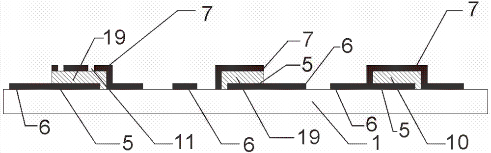
[0032] Such as Figure 7 As shown, the structure of the above-mentioned MEMS thin-film capacitive multi-parameter sensor is adopted in this embodiment, including: the carrier substrate 1 of the MEMS device, the MEMS thin-film capacitive pressure sensor 2, the MEMS thin-film capacitive temperature sensor 3, the MEMS thin-film capacitive sensor The humidity sensor 4 ; the above three sensors are arranged side by side on the carrier substrate 1 .

[0033] Such as Figure 7 As shown, the MEMS thin film capacitive pressure sensor 2 is provided with an upper electrode 7 and a lower electrode 5, and the upper and lower electrodes form a parallel plate capacitance structure; The cavity 8 of the pressure sensor 2; the cavity 8 is sealed with a film by the sealing layer 13, so that the air pressure value in the cavity 8 remains constant; the lower electrode 5 is arranged on the...


PUM

PropertyMeasurementUnit
thicknessaaaaaaaaaa
thicknessaaaaaaaaaa
thicknessaaaaaaaaaa

Abstract

The invention discloses an MEMS (Micro Electro Mechanical System) film capacitive type multi-parameter sensor structure and an integrated manufacturing method thereof. An MEMS carrying substrate is provided with MEMS film capacitive type pressure, temperature and humidity sensors which are arranged side by side. Electrodes, sacrificial layers, sensitive layers, sensitive films and protective layers of the three sensors adopt mutually matching structures and materials and therefore can be manufactured through an integrated surface micro-processing technology. The multi-parameter sensor structure and the integrated manufacturing method provided by the invention have the advantages of reducing volume of components, simplifying technical steps and being capable of decreasing cost of sensor products to a certain extent. In addition, the wholly capacitive structure adds application potential of the MEMS film capacitive type multi-parameter sensor structure in an inductive coupling based passive wireless sensing system.

Description

technical field [0001] The invention relates to a MEMS film capacitive multi-parameter sensor structure and an integrated manufacturing method thereof, belonging to the field of MEMS sensor manufacturing. Background technique [0002] With the development of Internet of Things technology, a large number of sensors are required to collect different types of data. Therefore, the production of MEMS sensors using batch micro-nano manufacturing technology plays an important role in improving the consistency of sensor performance and reducing the energy consumption of sensor systems and sensor costs. meaning. In particular, in production and life, on the one hand, people usually pay attention to multiple parameters in the measured environment at the same time (such as: pressure, temperature, humidity, chemical composition, etc.), therefore, it is necessary to use different sensors to collect sensitive parameters separately , in order to achieve process consistency, system miniatu...

Claims


Application Information

Patent Timeline
Patent Type & Authority Patents(China)
IPC IPC(8): G01D5/12B81B7/00B81C1/00
Inventor 秦毅恒欧文
Owner 中科芯未来微电子科技成都有限公司
Why Eureka
Try Eureka