
Multilayer ceramic substrate integrated waveguide filter

A substrate-integrated waveguide and multi-layer ceramic technology, which is applied to waveguide devices, electrical components, circuits, etc., can solve the problems of large size and achieve the effects of mass production, simple manufacturing process, and reduced circuit board area

Inactive Publication Date: 2012-11-28
UNIV OF ELECTRONICS SCI & TECH OF CHINA
View PDF0 Cites 26 Cited by
  • Summary
  • Abstract
  • Description
  • Claims
  • Application Information

AI Technical Summary

Problems solved by technology

[0005] The purpose of the present invention is to overcome the shortcomings of the existing multilayer ceramic substrate integrated waveguide filter, and propose a multilayer ceramic substrate integrated waveguide filter

Method used


Image

  • Multilayer ceramic substrate integrated waveguide filter
  • Multilayer ceramic substrate integrated waveguide filter
  • Multilayer ceramic substrate integrated waveguide filter

Examples


Embodiment Construction

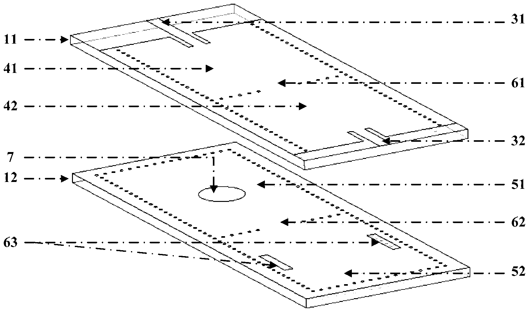
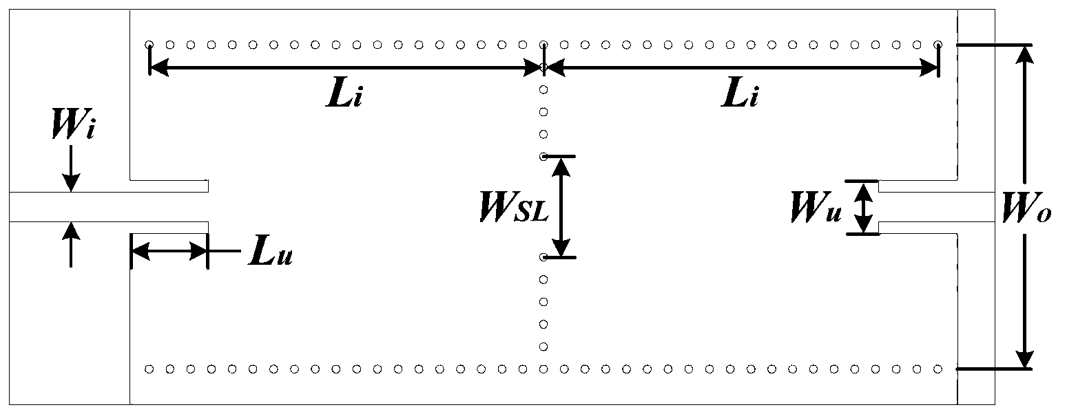
[0016] Below in conjunction with accompanying drawing and specific embodiment, the present invention will be further described: figure 1 and figure 2 As shown, the multilayer ceramic substrate integrated waveguide filter is a second-order bandpass filter with two transmission zeros, which is characterized in that it includes a third metal layer 23, a second metal layer stacked sequentially from bottom to top. The dielectric substrate 12, the second metal layer 22, the first dielectric substrate 11 and the first metal layer 21, the metallized via hole array 8 penetrates the first metal layer 21, the first dielectric substrate 11 and the second metal layer 22 and then Openings at both ends of the first dielectric substrate 11 (in the present invention, the incoherent metallized through hole array in the metal layer is regarded as an opening) form a first input and output terminal 41 and a second input and output terminal 42, the first The input and output ends 41 are connected...


PUM

PropertyMeasurementUnit
thicknessaaaaaaaaaa
diameteraaaaaaaaaa
frequencyaaaaaaaaaa

Abstract

The invention relates to a multilayer ceramic substrate integrated waveguide filter comprising a third metal layer, a second dielectric substrate, a second metal layer, a first dielectric substrate and a first metal layer which are sequentially stacked from the bottom up, wherein a metalized through-hole array runs through the first metal layer, the first dielectric substrate and the second metal layer and then forms a first input / output end and a second input / output end at the openings of two ends of the first dielectric substrate; the first input / output end is connected with a zonal first coplanar waveguide input / output structure; the second input / output end is connected with a zonal second coplanar waveguide input / output structure; and the common cavity wall of the first and second input / output end is provided with a first inductive coupling window introduction source load couple. The multilayer ceramic substrate integrated waveguide filter has the advantage and beneficial effect of being particularly suitable for system miniaturization and integrated application.

Description

technical field [0001] The invention belongs to the field of microwave and millimeter wave technology, in particular to a multilayer substrate integrated waveguide filter based on low temperature co-fired ceramic technology. Background technique [0002] The filter is one of the important passive components in the system, and its performance directly affects the selectivity, noise figure, gain and sensitivity of the system as a whole. Metal cavity filters usually have the advantages of low loss, high Q value, and good selectivity, but their processing is difficult, costly, bulky, and difficult to integrate with active circuits. Filters based on substrate-integrated waveguide technology not only have excellent performance similar to metal waveguide filters, but also are easy to process and planarly integrated, and have been widely researched and applied at present. As the system's requirements for circuit volume and weight become more stringent, higher requirements are also ...

Claims


Application Information

Patent Timeline
Patent Type & Authority Applications(China)
IPC IPC(8): H01P1/203H01P1/208
Inventor 徐自强徐美娟夏红廖家轩尉旭波
Owner UNIV OF ELECTRONICS SCI & TECH OF CHINA
Learn More