Manufacturing method for high-pressure quick soft recovery diode with diffusing buffer layer

A recovery diode and manufacturing method technology, applied in semiconductor/solid-state device manufacturing, electrical components, circuits, etc., can solve the problems of voltage drop increase, voltage drop, loss of conductance modulation ability, etc., and achieve soft recovery characteristics and cost reduction.

Active Publication Date: 2012-12-12
TSINGHUA UNIV +1
View PDF2 Cites 18 Cited by
  • Summary
  • Abstract
  • Description
  • Claims
  • Application Information

AI Technical Summary

Problems solved by technology

[0016] In the second case, the base width is limited to N + edge, no buffer
If the concentration is too low, or the width is too narrow, the space charge region will break through, the voltage will drop severely, and the buffering effect will not be achieved; if the concentration is too high, the recombination will be too fast, and the buffer layer will also not be able to function, and the buffering effect will also be lost. Conductance modulation capability, enabling voltage drop increases

Method used


Image

  • Manufacturing method for high-pressure quick soft recovery diode with diffusing buffer layer
  • Manufacturing method for high-pressure quick soft recovery diode with diffusing buffer layer
  • Manufacturing method for high-pressure quick soft recovery diode with diffusing buffer layer

Examples


Embodiment Construction

[0046] The invention proposes a manufacturing method of a high-voltage fast soft recovery diode with a diffusion buffer layer. Be described below in conjunction with accompanying drawing.

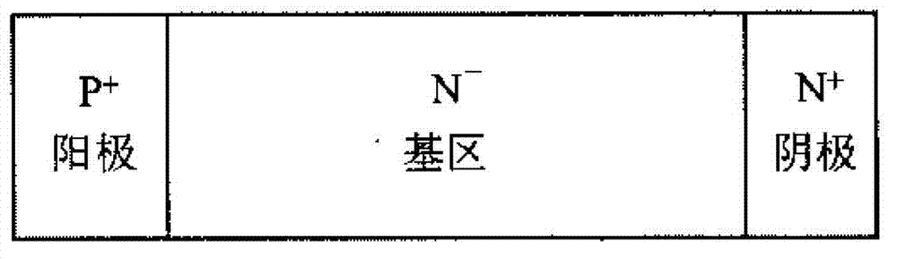
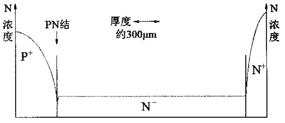
[0047] So far, buffer layers for fast recovery diodes have all been fabricated using a two-step epitaxy method. The main production steps are as follows: the raw material is silicon single crystal N + Substrate sheet, sheet thickness 500-600μm, doping concentration> 8×10 19 cm -3 ; at N + A thin layer with a concentration of 10 was grown on the substrate by epitaxy 14 cm -3 The range of silicon single crystal film is used as N buffer layer; then continue to epitaxially grow N on the N buffer layer - single crystal layer for diode N - Base and P + layer production.

[0048] The existing problems of making fast recovery diodes by epitaxial method are: 1. In view of the current technical level of epitaxial technology, the thickness of the epitaxial layer can only be up to 100 μm, whic...


PUM


Abstract

The invention discloses a manufacturing method for a high-pressure quick soft recovery diode with a diffusing buffer layer and belongs to the field of semiconductor devices. A buffer layer of a quick recovery diode with the diffusing buffer layer is manufactured by adopting a twice diffusing method. Before a PN junction and an electrode are prepared, the primary phosphorus diffusing is firstly adopted so as to generate low-concentration and high-junction-depth phosphorus diffusing areas on two surfaces of a silicon wafer, and then the junction depth of the primary phosphorus diffusing is continuously boosted during the processes of secondary phosphorus diffusing and boron aluminum diffusing, and lastly, the junction depth of the primary phosphorus diffusing is 20 microns deeper than that of the secondary phosphorus diffusing and the depth of the area with a front concentration less than 1*1015/cm-3 of the primary phosphorus diffusing is not less than 15 microns. A defect zone-free silicon-melted single crystal and the diffusing buffer layer are adopted, so that the voltage and current levels of the quick soft recovery diode are greatly increased.

Description

technical field [0001] The invention belongs to the scope of semiconductor devices, in particular to a manufacturing method of a high voltage (1600V) fast soft recovery diode with a diffusion buffer layer. Background technique [0002] The basic structure of a diode is a PN junction (as attached figure 1 , 2 shown), but in order to lead out the electrode, a high-concentration P+ and N+ layer must be introduced at the contact part of the electrode and the semiconductor material to ensure ohmic contact and reduce ohmic contact resistance. It can be understood from the working principle of the diode: [0003] 1) In the forward direction, that is, at the anode of the diode (P + ) is connected to the "+" pole of the external circuit, and the cathode (N + ) is terminated with "-" pole, under the action of electric field, P + end will be to N - The base region injects a large number of positively charged minority carriers—holes, N + End to N - The base injects a large number...

Claims


Application Information

Patent Timeline
Patent Type & Authority Applications(China)
IPC IPC(8): H01L21/329H01L21/225
Inventor 周伟松刘道广张斌王培清
Owner TSINGHUA UNIV
Why Eureka
Try Eureka