Nanometer silicon carbide/crystal silicon carbide double graded junction fast recovery diode and preparation method thereof

A nano-silicon carbide, fast recovery technology, applied in semiconductor/solid-state device manufacturing, semiconductor devices, electrical components, etc., can solve the problems of difficult adjustment of interface defects and difficult to accurately control reverse recovery performance indicators of reverse recovery current.

Active Publication Date: 2012-12-12
WEEN SEMICON TECH CO LTD
View PDF2 Cites 10 Cited by
  • Summary
  • Abstract
  • Description
  • Claims
  • Application Information

AI Technical Summary

Problems solved by technology

The existing Si and SiC material FRD is generally P + -N - -N + (Also known as P-I-N) type, due to the limitation of process conditions, P + , N + layer thickness and P + / N - Knot, N - / N + Junction interface defects are not easy to adjust, the peak value of reverse recovery current (I RRM ), t RR Reverse recovery performance indicators such as and S are difficult to accurately control

Method used


Image

  • Nanometer silicon carbide/crystal silicon carbide double graded junction fast recovery diode and preparation method thereof
  • Nanometer silicon carbide/crystal silicon carbide double graded junction fast recovery diode and preparation method thereof
  • Nanometer silicon carbide/crystal silicon carbide double graded junction fast recovery diode and preparation method thereof

Examples


Embodiment approach 1

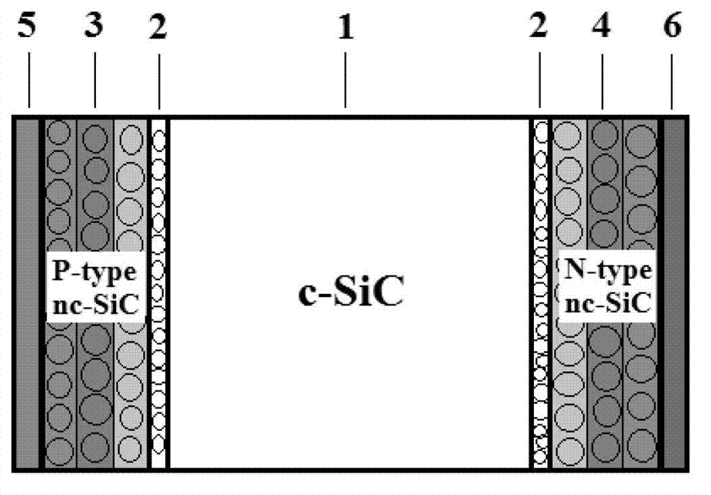
[0057] like figure 1 , the specific embodiment 1 of the product of the present invention, the thickness is about 50±2 μm, and the average carrier concentration range is 1.0×10 14 —9.0×10 14 cm -3 , double-sided polished N - The type 4H-SiC substrate is the substrate, the surface is the Si atomic plane, 8° away from the (0001) plane, and the surface micropipe density is lower than 30μP·cm -2 . Of course, the carrier concentration of the c-SiC substrate of the present invention can also be lower than 1.0×10 14 cm -3 , the thickness can be slightly thinner or thicker.

specific Embodiment approach 2

[0058] like figure 1 , the specific embodiment 2 of the product of the present invention is different from the embodiment 1 in the nc-Si thin film. On the left side of the 4H-SiC substrate, a layer of nc-Si thin film with a thickness of several nanometers is deposited. Smooth and tightly bonded.

specific Embodiment approach 3

[0059] like figure 1 , the specific embodiment 3 of the product of the present invention is different from the embodiment 1 and 2 in that the P-type nc-SiC multilayer film is described. 8-10 layers of P-type nc-SiC multi-layer films with a thickness of 0.05-0.08 μm and increasing boron doping deposited on the nc-Si ultra-thin film on the left side of the 4H-SiC substrate (note: the first layer may not Doping, that is, intrinsic), the nc-SiC grain is 4H-SiC type, and the carrier concentration of the multilayer film increases from 0 to 1.0×10 19 cm -3 . The nc-SiC film and 4H-SiC constitute P + P / N - Unilateral gradient heterogeneity structure.


PUM

PropertyMeasurementUnit
thicknessaaaaaaaaaa
thicknessaaaaaaaaaa
thicknessaaaaaaaaaa

Abstract

The invention discloses a nanometer silicon carbide / crystal silicon carbide double graded junction fast recovery diode and a preparation method thereof. The nanometer silicon carbide / crystal silicon carbide double graded junction fast recovery diode comprises a monocrystal silicon carbide (4H-SiC) substrate, number nanometer nc-Si ultra thin layers respectively arranged on two sides of the 4H-SiC substrate, P and N type gradient doping multilayer nc-SiC thin films (4H-SiC type) and an alloy ohmic electrode deposited on an outer layer nc-SiC thin film, and a gradient doping multilayer nc-SiC multilayer film, the 4H-SiC substrate and the alloy ohmic electrode form an electrode / nc-SiC / 4H-SiC / nc-SiC / electrode double graded junction structure. The nanometer silicon carbide / crystal silicon carbide double graded junction fast recovery diode has the advantages that, compared with fast recovery diodes (FRD) prepared by other methods, reverse breakdown voltage improves by about 500V, withstand voltage capacity is strengthened, reverse recovery time is shortened to 100nS, high-speed switch is easy to achieve, surge current during reverse recovery is small, and loss and electromagnetic interference are reduced.

Description

technical field [0001] The invention belongs to the technical field of power electronics, and relates to semiconductor devices, specifically a fast recovery diode (FRD for short), more specifically nanometer silicon carbide (nc-SiC) / single crystal silicon carbide (c-SiC) -SiC) preparation method of double slow-junction fast recovery diode, and FRD obtained by this method. Background technique [0002] FRD is a diode that can be turned on and off quickly. It is usually used in conjunction with three-terminal power switching devices such as insulated gate-gated bipolar transistors (IGBTs) and integrated gate commutated thyristors (IGCTs) to turn on the load. The reactive current can shorten the charging time of the capacitor, and suppress the high voltage induced by the instantaneous reversal of the load current. It is widely used in power electronics and communication equipment such as AC-DC converters and pulse width modulators. [0003] FRDs of existing crystalline silic...

Claims


Application Information

Patent Timeline
Patent Type & Authority Applications(China)
IPC IPC(8): H01L29/06H01L29/861H01L21/329
Inventor 韦文生
Owner WEEN SEMICON TECH CO LTD
Why Eureka
Try Eureka