Photoelectric detection lamination, semiconductor ultraviolet detector and manufacturing method of semiconductor ultraviolet detector

An ultraviolet detector and photoelectric detection technology, which is applied in the direction of semiconductor devices, final product manufacturing, sustainable manufacturing/processing, etc., can solve the problems of high manufacturing cost and low photoelectric efficiency, achieve enhanced photogenerated current, reduce manufacturing cost, and enhance The effect of the photoelectric effect

Active Publication Date: 2012-12-19
INST OF MICROELECTRONICS CHINESE ACAD OF SCI
View PDF5 Cites 5 Cited by
  • Summary
  • Abstract
  • Description
  • Claims
  • Application Information

AI Technical Summary

Problems solved by technology

[0006] However, the photoelectric detection materials used in the above-mentioned existing semiconductor ultraviolet detectors are in polycrystalline or crystalline states, the manufacturing cost is high, and the photoelectric efficiency is low. However, with the improvement of detection application requirements, the photoelectric efficiency has also been raised. higher requirement

Method used


Image

  • Photoelectric detection lamination, semiconductor ultraviolet detector and manufacturing method of semiconductor ultraviolet detector
  • Photoelectric detection lamination, semiconductor ultraviolet detector and manufacturing method of semiconductor ultraviolet detector
  • Photoelectric detection lamination, semiconductor ultraviolet detector and manufacturing method of semiconductor ultraviolet detector

Examples


Embodiment 1

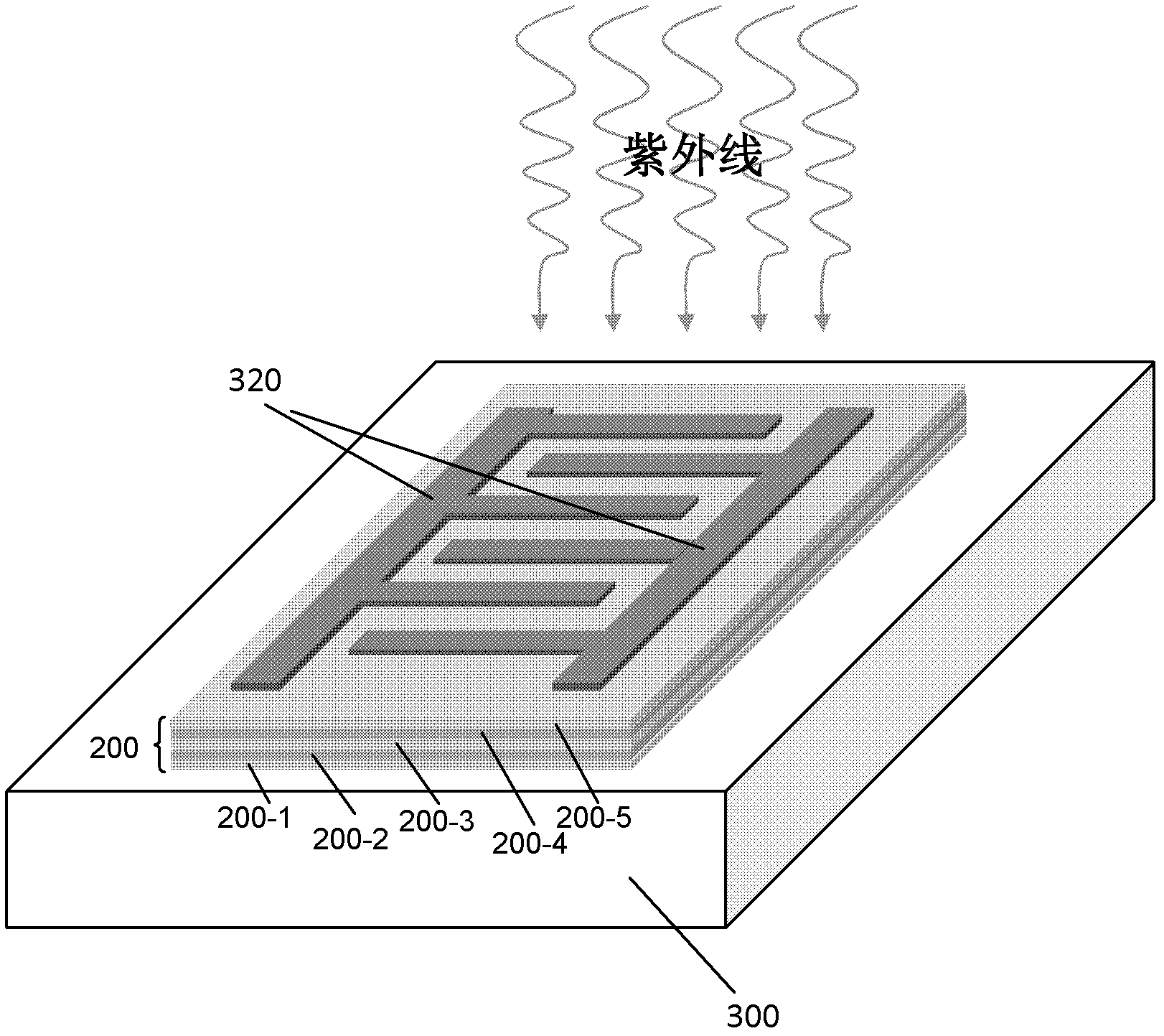
[0052] In this embodiment, a semiconductor ultraviolet detector with an MSM structure of the above-mentioned photodetection stack is provided, referring to image 3 As shown, the detectors include:

[0053] substrate 300;

[0054] a photodetection stack 200 on a substrate 300;

[0055] an electrode 320 on the photodetection stack 200;

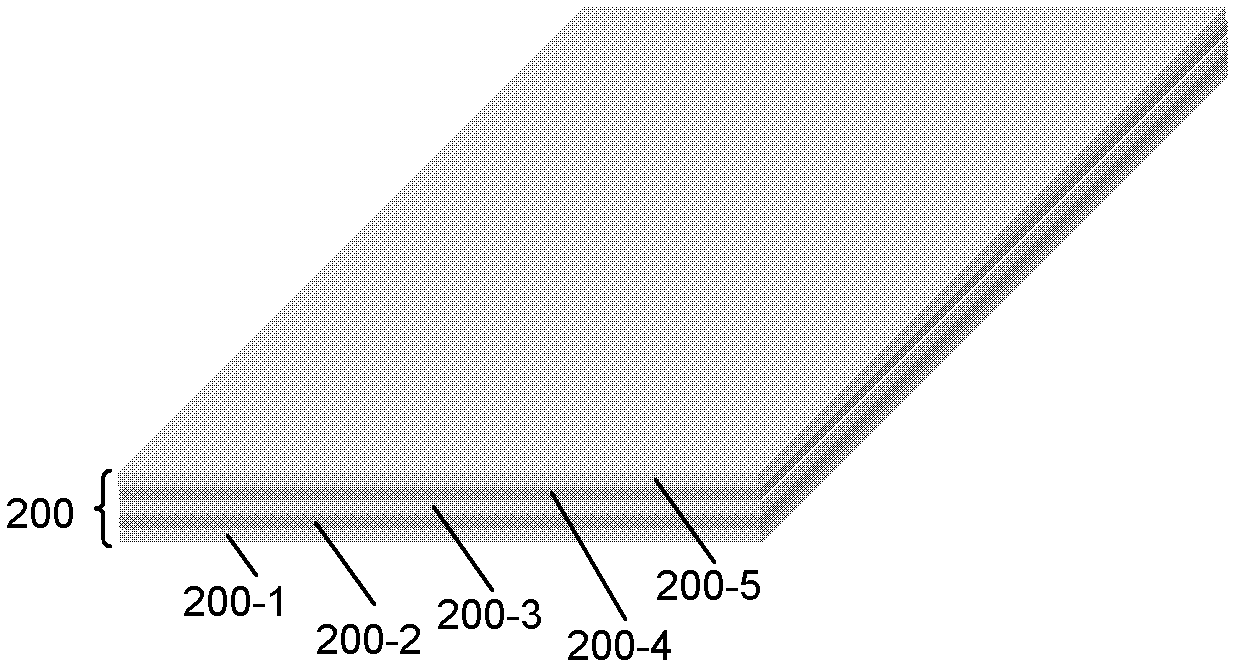
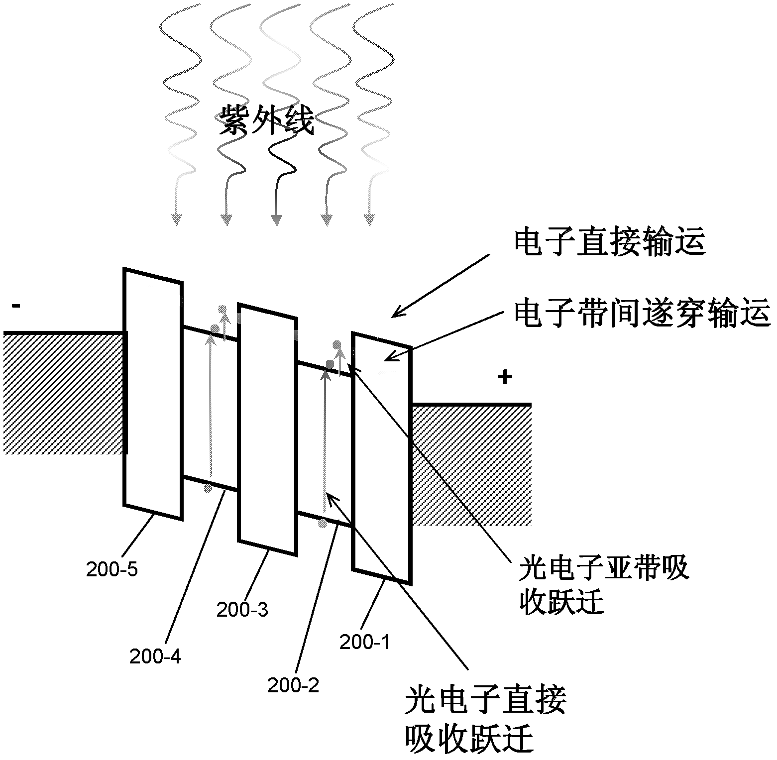
[0056] Wherein, the photodetection stack includes m layers of wide-bandgap amorphous oxide semiconductor layers and n layers of narrow-bandgap amorphous oxide semiconductor layers, and the wide-bandgap amorphous oxide semiconductor layer and narrow-bandgap The amorphous oxide semiconductor layers are arranged alternately, the forbidden band width of the wide bandgap amorphous oxide semiconductor layer is larger than the narrow bandgap amorphous oxide semiconductor layer, m, n≥1 .

[0057] It should be noted that, in this embodiment, all the content of the photodetection stack refers to the description in the above-mentioned photodetection s...

Embodiment 2

[0073] In this embodiment, a semiconductor ultraviolet detector with a TFT structure of the above-mentioned photodetection stack is provided, referring to Figure 4 , the detectors include:

[0074] substrate 300;

[0075] a gate electrode 310 on the substrate 300;

[0076] The gate electrode 310 and the gate insulating layer 312 on the substrate 300 on both sides of the gate electrode;

[0077] the photodetection stack 200 on the gate insulating layer 312;

[0078] Source / drain electrodes 320 on the photodetection stack 200 on both sides of the gate electrode 310;

[0079] Wherein, the photodetection stack includes m layers of wide-bandgap amorphous oxide semiconductor layers and n layers of narrow-bandgap amorphous oxide semiconductor layers, and the wide-bandgap amorphous oxide semiconductor layer and narrow-bandgap The amorphous oxide semiconductor layers are arranged alternately, the forbidden band width of the wide bandgap amorphous oxide semiconductor layer is large...


PUM


Abstract

The embodiment of the invention discloses a photoelectric detection lamination. The photoelectric detection lamination comprises m broad-band gap amorphous oxide semiconductor layers, n narrow-band gap amorphous oxide semiconductor layers, and an electrode on the photoelectric detection lamination, wherein the broad-band gap amorphous oxide semiconductor layers and the narrow-band gap amorphous oxide semiconductor layers are alternately arranged, the forbidden band width of the broad-band gap amorphous oxide semiconductor layers is greater than the forbidden band width of the narrow-band gap amorphous oxide semiconductor layers, and m and n are not less than 1. Through the formed photoelectric detection lamination with amorphous oxide semiconductors with high and low staggered energy bands, photo-generated current is increased and photoelectric efficiency is greatly improved.

Description

technical field [0001] The invention relates to semiconductor manufacturing technology, more specifically, to a photodetection stack, a semiconductor ultraviolet detector and a manufacturing method thereof. Background technique [0002] In recent years, with the continuous deepening of research and exploration in the fields of astronomy, high-energy physics, and space technology, higher requirements have been put forward for ultraviolet detection technology and detection materials. Ultraviolet (UV) detection technology is another dual-use photoelectric detection technology developed after infrared and laser detection technology, which has high application value in both military and civilian applications. In the military, ultraviolet detection technology can be used in missile guidance, missile early warning, ultraviolet communication, ultraviolet interference, photoelectric countermeasures and other fields, which have attracted great attention from the military. In the civi...

Claims


Application Information

Patent Timeline
Patent Type & Authority Applications(China)
IPC IPC(8): H01L31/0352H01L31/112H01L31/18
CPCY02P70/50
Inventor 殷华湘陈大鹏
Owner INST OF MICROELECTRONICS CHINESE ACAD OF SCI
Why Eureka
Try Eureka