

Adhesive-removal method for printed circuit board HDI (high density interconnection) product
A technology of printed circuit boards and products, which is applied in the direction of printed circuit, printed circuit manufacturing, electrical components, etc., and can solve problems such as batch scrapping and blind hole opening
Active Publication Date: 2012-12-19
东莞市若美电子科技有限公司
View PDF6 Cites 25 Cited by
- Summary
- Abstract
- Description
- Claims
- Application Information
AI Technical Summary
Problems solved by technology
In the actual production process, the abnormal thickness control of the blind hole dielectric layer and the abnormal laser drilling often have a great impact on the subsequent glue removal. The traditional vertical glue removal (chemical potion) method cannot completely solve the problem of resin residue at the bottom of the blind hole. Cause blind holes to open, leading to batch scrap
Method used
View moreImage
Smart ImageViewing Examples

Examples
Embodiment 2
[0043] Embodiment three:
Embodiment 3
[0045] The above content is only a preferred embodiment of the present invention. For those of ordinary skill in the art, according to the idea of the present invention, there will be changes in the specific implementation and application scope. limits.
Login to View More PUM
 Abstract
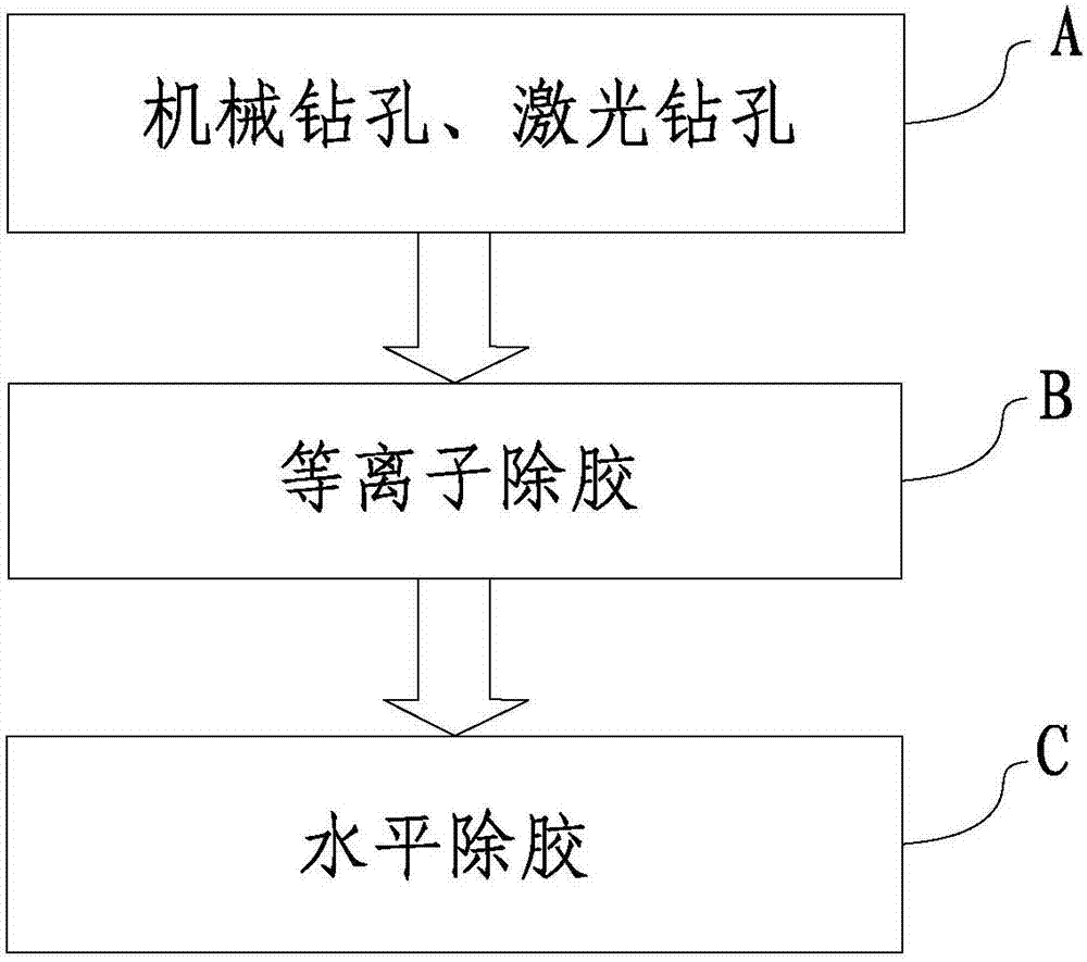
The invention relates to the technical field of the printed circuit board, in particular to an adhesive-removal method for a printed circuit board HDI (high density interconnection) product. The adhesive-removal method comprises the following steps of: A) mechanical drilling and laser drilling: carrying out mechanical drilling on an HDI product, and carrying out laser drilling on the HDI product to form a through hole and a blind hole; B) plasma adhesive removal: generating a plasma by oxygen and carbon tetrafluoride under the action of the nitrogen environment and an RF electric field, and enabling the plasma to react with resin on the walls of the through hole and the blind hole to generate carbon dioxide, hydrogen fluoride and water; and C) horizontal adhesive removal: processing the through hole and the blind hole by chemical potion in a horizontal adhesive removal method. Firstly, the blind hole and the through hole are subjected to the plasma adhesive removal, the generated carbon dioxide, hydrogen fluoride and water can be absorbed without residuals in the blind hole, and then the blind hole and the through hole are subjected to horizontal adhesive removal to effectively remove tiny residual adhesives on the bottom of the blind hole and clean the blind hole.
Description
technical field [0001] The invention relates to the technical field of printed circuit boards, in particular to a method for removing glue from printed circuit board HDI products. Background technique [0002] HDI is the abbreviation of High Density Interconnection (High Density Interconnection), a technology for producing printed circuit boards, a circuit board with a relatively high circuit distribution density using micro-blind buried hole technology. HDI is a compact product designed for small-capacity users. The dielectric layer (prepreg) after multilayer board lamination itself contains a certain amount of resin, which is the glue that needs to be removed by this technical method. With the continuous development of traditional HDI and system HDI product technology, blind hole dielectric layer thickness uniformity control technology, laser drilling technology, descaling copper plating technology have a great impact on the reliability of blind holes. In the actual produ...
Claims
Login to View More Application Information
Patent Timeline
 IPC IPC(8): H05K3/00
Inventor张文昌洪少鸿
Owner东莞市若美电子科技有限公司