Preparation method for silicon-based nanometer array patterned substrate and silicon-based epitaxial layer
A patterned substrate and silicon nano-array technology, applied in semiconductor/solid-state device manufacturing, electrical components, circuits, etc., can solve the problems of high cost and complicated process, and achieve low cost, simple preparation process, and high crystal quality Effect
- Summary
- Abstract
- Description
- Claims
- Application Information
AI Technical Summary
Problems solved by technology
Method used
Image

Examples
Embodiment 1
[0034] As shown in the figure, this embodiment provides a method for preparing a silicon-based nanoarray patterned substrate, including the following steps:
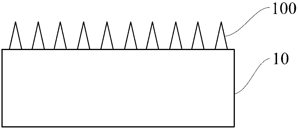
[0035] First, if figure 1 As shown, in step 1, a silicon substrate 10 is provided, and the crystal plane of the silicon substrate 10 is (100). Since the crystal orientation of the film must best match the crystal orientation of the surface of the silicon substrate 10 to be epitaxial, in the subsequent When Ge is epitaxially grown on the (100) crystal plane of the silicon substrate 10, it is more conducive to releasing the tensile stress, but it is not limited thereto, and other crystal planes of silicon can also be used in other embodiments; then the silicon substrate 10 is placed into the predetermined concentration of AgNO 3 The silicon substrate 10 with the silicon nano-array 100 is formed by chemical catalytic etching in a mixed solution of HF and HF. During etching, a certain amount of ammonium fluoride can be adde...
Embodiment 2
[0044] As shown in the figure, this embodiment provides a method for preparing a silicon-based epitaxial layer, including the following steps:
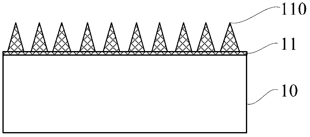
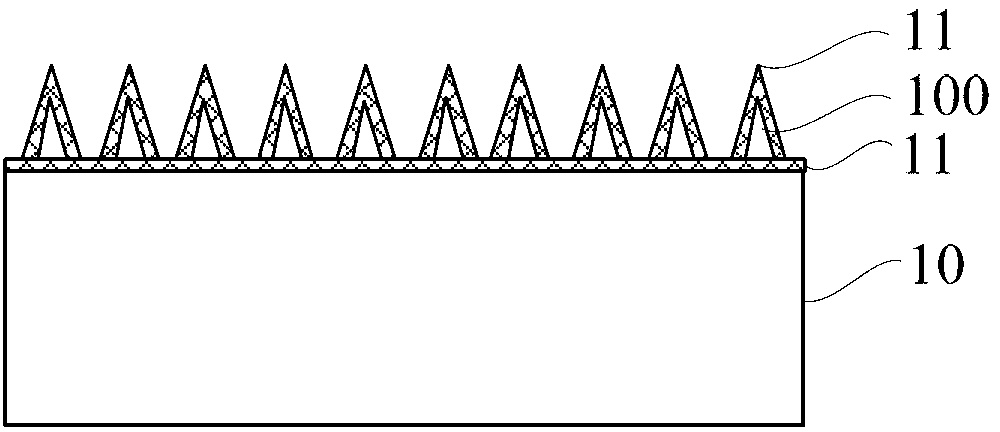
[0045] Step 1: Using the method described in Embodiment 1 of the present invention to prepare a silicon-based nanoarray patterned substrate, the specific process will not be described in detail in this embodiment, and the specific process diagram refers to Embodiment 1 figure 1 ,, Figure 2a-2b ,as well as Figure 3a~3b .
[0046] Step 2: growing an epitaxial layer 12 on the silicon-based nano-array patterned substrate by using a selective epitaxy process. The selective epitaxy process is a common method used by those skilled in the art and will not be repeated here. In this implementation, the epitaxial layer 12 is temporarily selected as a Ge layer, but it is not limited thereto. In other embodiments, the parameters of the preparation process of the silicon-based nanoarray patterned substrate and the parameters of the epitaxial pr...
PUM
 Abstract
Description
Claims
Application Information
 - Generate Ideas
- Intellectual Property
- Life Sciences
- Materials
- Tech Scout
- Unparalleled Data Quality
- Higher Quality Content
- 60% Fewer Hallucinations
Browse by: Latest US Patents, China's latest patents, Technical Efficacy Thesaurus, Application Domain, Technology Topic, Popular Technical Reports.
© 2025 PatSnap. All rights reserved.Legal|Privacy policy|Modern Slavery Act Transparency Statement|Sitemap|About US| Contact US: help@patsnap.com