Three-dimensional packaging device for photonic integrated chip matching circuit

A technology of photon integration and matching circuits, applied in circuits, optical multiplexing systems, optics, etc., can solve the problems of increasing circuit design dimensions and matching circuit size limitations, and achieve impedance matching, enhanced heat dissipation, and heat dissipation The effect of area enlargement

Active Publication Date: 2013-01-02
INST OF SEMICONDUCTORS - CHINESE ACAD OF SCI
View PDF3 Cites 13 Cited by
  • Summary
  • Abstract
  • Description
  • Claims
  • Application Information

AI Technical Summary

Problems solved by technology

[0006] In view of this, the main purpose of the present invention is to provide a three-dimensional packaging device for photonic integrated chip matching circuits, to overcome the problem of limited matching circuit size caused by the limitation of array chip spacing when packaging photonic integrated chip arrays, and to break through the microwave circuit. The traditional design is only limited by the two-dimensional plane, which increases the dimension of the circuit design and reserves space for the design of microwave circuits

Method used


Image

  • Three-dimensional packaging device for photonic integrated chip matching circuit
  • Three-dimensional packaging device for photonic integrated chip matching circuit
  • Three-dimensional packaging device for photonic integrated chip matching circuit

Examples


Embodiment Construction

[0032] In order to make the object, technical solution and advantages of the present invention clearer, the present invention will be described in further detail below in conjunction with specific embodiments and with reference to the accompanying drawings.

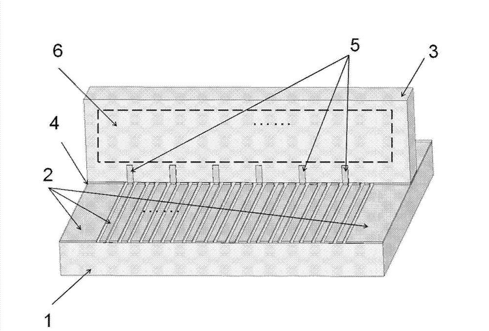
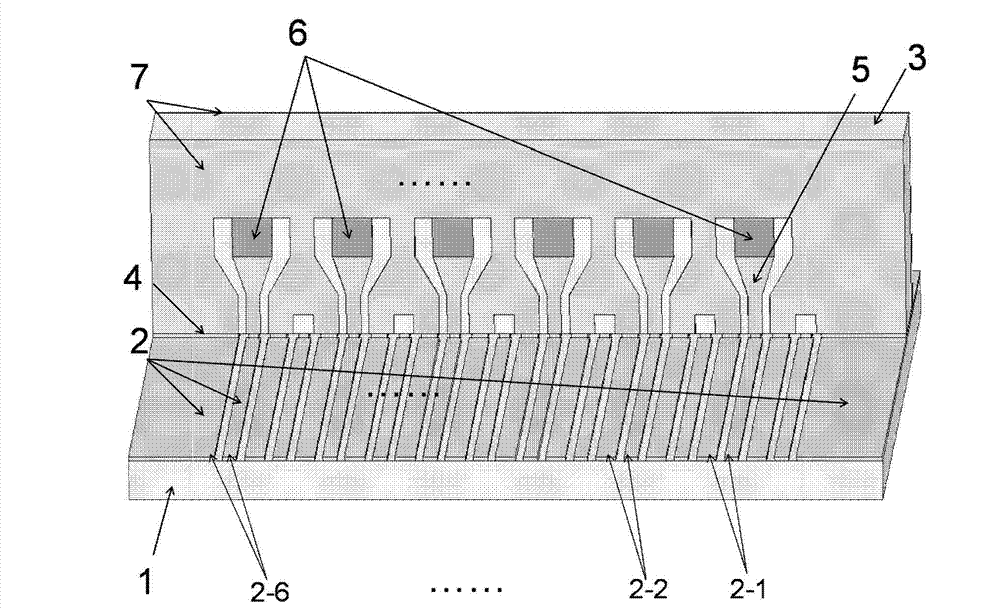
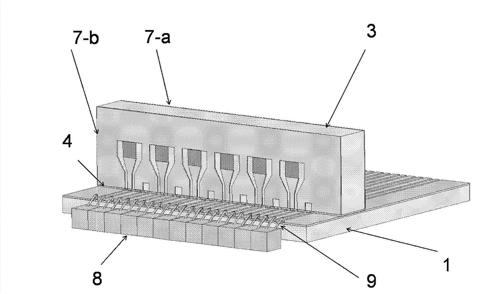
[0033] Such as figure 1 as shown, figure 1 It is a structural schematic diagram of a three-dimensional packaging device for a photonic integrated chip matching circuit provided by the present invention. The device includes: a first carrier substrate 1; a first microwave transmission line array 2 evaporated on the first carrier substrate 1 The surface is used to provide bias voltage and high-frequency modulation signal to the photonic integrated chip; a second carrier substrate 3 is perpendicular to or at a certain angle with the first carrier substrate 1 to form a three-dimensional structure; a second microwave transmission line An array 4 is vapor-deposited on the lower surface of the second carrier substrate 3, and is ...


PUM


Abstract

The invention discloses a three-dimensional packaging device for a photonic integrated chip matching circuit. The three-dimensional packaging device comprises a first carrier substrate, a first microwave transmission line array, a second carrier substrate, a second microwave transmission line array, an electrode array and a microwave circuit, wherein the first microwave transmission line array is evaporated on the upper surface of the first carrier substrate and used for providing bias voltage and high-frequency modulating signals for photonic integrated chips; the second carrier substrate is perpendicular to the first carrier substrate or forms a certain angle with the same so that a three-dimensional stereoscopic structure is formed; the second microwave transmission line array is evaporated on the lower surface of the second carrier substrate and is matched with an electrode of the first microwave transmission line array by welding or sintering; and the electrode array is evaporated on one side face or two opposite side faces of the second carrier substrate. The three-dimensional packaging device for the photonic integrated chip matching circuit solves the problem that a matching circuit is limited in size due to limitation on array chip spacing during integrated chip array packaging and breaks through limitations that a microwave circuit is just in a two-dimensional plane in traditional design, dimensionality of circuit design is increased, and space for designing the microwave circuit is reserved.

Description

technical field [0001] The invention belongs to the field of optoelectronic devices, in particular to a three-dimensional packaging device for photonic integrated chip matching circuits. Background technique [0002] At present, optical network equipment constructed by discrete optoelectronic devices is difficult to adapt to the rapidly developing optical fiber communication network. Photonic integrated chip (PIC) is a technology that must be relied on to realize large-capacity and low-power optical networks. In order to effectively load the external microwave signal to the photonic integrated chip, the transitional heat sink is required to have an impedance matching microwave circuit with high efficiency, low reflection and low loss. [0003] Significantly different from discrete devices, ultra-high integration reduces the scale of integrated devices to the micro-nano level, which puts forward stricter requirements for the development and packaging of devices. The circuit ...

Claims


Application Information

Patent Timeline
Patent Type & Authority Applications(China)
IPC IPC(8): H01L23/58H01L23/66H01L23/367
CPCH01L2924/0002H01Q13/206H01L23/58H01L2224/48091H01P11/003G02B6/00H04J14/00H01P1/36H01L2224/45144H01L23/66G02F1/0121H01L2924/00014H01L2924/00
Inventor 祝宁华王佳胜刘建国刘宇
Owner INST OF SEMICONDUCTORS - CHINESE ACAD OF SCI
Why Eureka
Try Eureka