Transient voltage suppressor and application thereof
A technology of transient voltage suppression and injection area, which is applied in the direction of electric solid-state devices, circuits, electrical components, etc., can solve problems such as difficult ESD protection, high trigger voltage, and small application range, and achieve good ESD clamping characteristics, conduction Small on-resistance and strong ESD conduction capability
- Summary
- Abstract
- Description
- Claims
- Application Information
AI Technical Summary
Problems solved by technology
Method used
Image

Examples
Embodiment 1
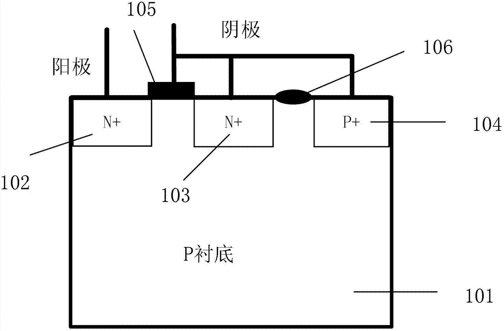
[0035] Such as image 3 and Figure 5 As shown, a transient voltage suppressor includes a P substrate 10;
[0036] N well 20, first N+ active injection region 31 and first P+ active injection region 41 are embedded on P substrate 10; second N+ active injection region 32 and second P+ active injection region 41 are embedded on N well 20. a source implantation region 42; a third N+ active implantation region 33 is embedded at the junction of the P substrate 10 and the N well 20;
[0037] The second P+ active injection region 42 is adjacent to the second N+ active injection region 32 and the third N+ active injection region 33; the first N+ active injection region 31 is adjacent to the third N+ active injection region 33 and the first The P+ active injection region 41 is adjacent to the left and right;
[0038] A gate region 5 is provided on the P substrate 10 between the first N+ active implant region 31 and the third N+ active implant region 33, and the first N+ active impla...
Embodiment 2
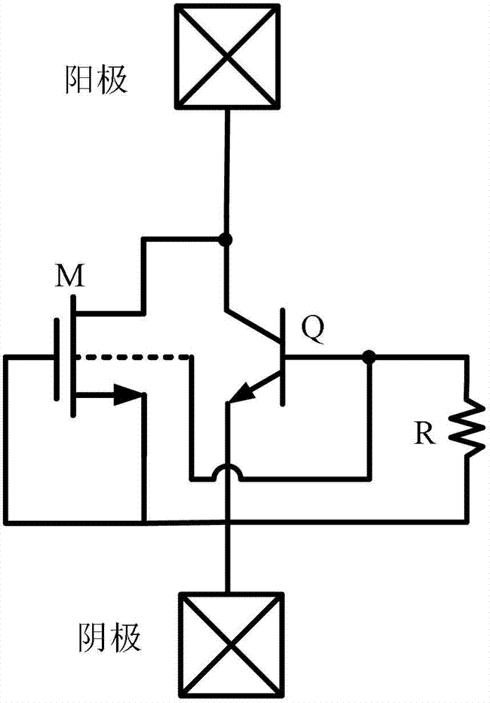
[0051] Such as Figure 7 As shown, a finger-type transient voltage suppressor includes two transient voltage suppressors as described in Embodiment 1; two transient voltage suppressors share a P substrate, and two transient voltage suppressors The anodes are connected together as the anode of the finger-type transient voltage suppressor, and the cathodes of the two transient voltage suppressors are connected together as the cathode of the finger-type transient voltage suppressor.
[0052] The finger-type transient voltage suppressor can further enhance the ESD current conduction capability of the device; it is manufactured under the 0.35um standard CMOS process, through Figure 8 It can be seen from the measured experimental data that the ESD current conduction capability of two interfinger transient voltage suppressors is stronger than that of a single transient voltage suppressor, the trigger voltage and sustain voltage of the device remain basically unchanged, and the curre...
PUM
| Property | Measurement | Unit |
|---|---|---|
| Width | aaaaa | aaaaa |
Abstract
Description
Claims
Application Information
 - R&D
- Intellectual Property
- Life Sciences
- Materials
- Tech Scout
- Unparalleled Data Quality
- Higher Quality Content
- 60% Fewer Hallucinations
Browse by: Latest US Patents, China's latest patents, Technical Efficacy Thesaurus, Application Domain, Technology Topic, Popular Technical Reports.
© 2025 PatSnap. All rights reserved.Legal|Privacy policy|Modern Slavery Act Transparency Statement|Sitemap|About US| Contact US: help@patsnap.com