Semiconductor device and manufacturing method thereof

A manufacturing method and semiconductor technology, applied in semiconductor/solid-state device manufacturing, semiconductor devices, transistors, etc., can solve problems such as changes in conductivity of oxide semiconductors

Active Publication Date: 2013-01-02
SEMICON ENERGY LAB CO LTD
View PDF7 Cites 4 Cited by
  • Summary
  • Abstract
  • Description
  • Claims
  • Application Information

AI Technical Summary

Problems solved by technology

[0006] However, the conductivity of the oxide semiconductor may change when hydrogen that forms an electron donor, the incorporation of moisture, etc., occur in the process of forming the device

Method used


Image

  • Semiconductor device and manufacturing method thereof
  • Semiconductor device and manufacturing method thereof
  • Semiconductor device and manufacturing method thereof

Examples


Embodiment approach 1

[0079] In this embodiment, an embodiment of a semiconductor device and a method of manufacturing the semiconductor device will be described with reference to FIGS. 1A to 3D. In this embodiment, a transistor having an oxide semiconductor film is shown as an example of a semiconductor device.

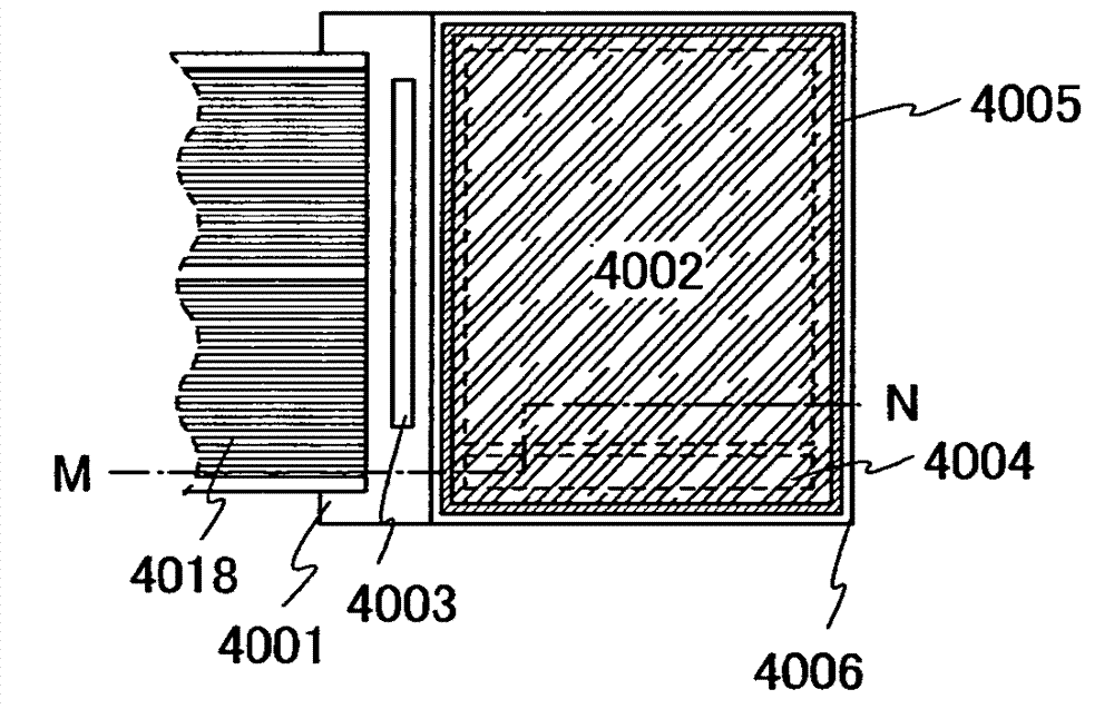
[0080] As an example of a semiconductor device, a cross-sectional view and a plan view of a bottom-gate transistor are shown in FIGS. 1A to 1C. Fig. 1A is a plan view, and Figs. 1B and 1C are cross-sectional views taken along line A-B and line C-D in Fig. 1A, respectively. Note that in FIG. 1A, the gate insulating film 402 is omitted.

[0081] The transistor 410 shown in FIGS. 1A, 1B, and 1C includes a gate electrode layer 401, a gate insulating film 402, an oxide semiconductor film 403, a source electrode layer 405a, and a drain electrode layer 405b on a substrate 400 having an insulating surface.

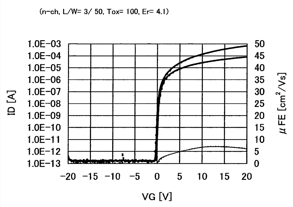
[0082] In the manufacturing process of the oxide semiconductor film 403, heat treatment and ox...

Embodiment approach 2

[0160] In this embodiment, another embodiment of the semiconductor device and one embodiment of the method of manufacturing the semiconductor device will be described with reference to FIGS. 4A to 4F and FIGS. 5A to 5C. In this embodiment, a transistor having an oxide semiconductor film is shown as an example of a semiconductor device. The same parts or parts with the same functions as those described in Embodiment Mode 1 can be performed similarly to those in Embodiment Mode 1, and repeated descriptions are omitted. In addition, detailed descriptions of the same parts are omitted.

[0161] An example of a method of manufacturing the transistor 450 is shown in FIGS. 4A to 4F and FIGS. 5A to 5C. In this embodiment, the oxygen doping treatment is performed multiple times in the manufacturing process of the transistor 450.

[0162] First, after forming a conductive film on the substrate 400 having an insulating surface, the gate electrode layer 401 is formed through a first photolit...

Embodiment approach 3

[0215] In this embodiment, another embodiment of the semiconductor device will be described with reference to FIGS. 13A to 13D. The same part or a part having a similar function as the part described in Embodiment 1 or 2 can be formed in a similar manner to that described in Embodiment 1 or 2, and repeated description is omitted. In addition, detailed descriptions of the same parts are omitted.

[0216] In this embodiment, an example of a structure in which a conductive layer (wiring layer, pixel electrode layer, etc.) is connected to the source electrode layer and / or drain electrode layer of a transistor is shown. In addition, this embodiment mode can also be applied to any of the transistors described in Embodiment Mode 1 and Embodiment 2.

[0217] As shown in FIG. 13A, the transistor 470 includes a gate electrode layer 401, a gate insulating film 402, an oxide semiconductor film 403, a source electrode layer 405a, and a drain electrode layer 405b on a substrate 400 having an in...


PUM


Abstract

A semiconductor device using an oxide semiconductor, with stable electric characteristics and high reliability. In a process for manufacturing a bottom-gate transistor including an oxide semiconductor film, dehydration or dehydrogenation is performed by heat treatment and oxygen doping treatment is performed. The transistor including the oxide semiconductor film subjected to the dehydration or dehydrogenation by the heat treatment and the oxygen doping treatment is a transistor having high reliability in which the amount of change in threshold voltage of the transistor by the bias-temperature stress test (BT test) can be reduced.

Description

Technical field [0001] The present invention relates to a semiconductor device and a manufacturing method of the semiconductor device. [0002] In this specification, semiconductor devices generally refer to all devices that can operate by utilizing semiconductor characteristics, and therefore electro-optical devices, semiconductor circuits, and electronic equipment are all semiconductor devices. Background technique [0003] The technology of forming a transistor using a semiconductor thin film formed on a substrate with an insulating surface has attracted attention. This transistor is widely used in electronic equipment such as integrated circuits (ICs) and image display devices (display devices). As a semiconductor thin film material that can be applied to transistors, silicon-based semiconductor materials are widely known. However, as other materials, oxide semiconductors are attracting attention. [0004] For example, a transistor has been disclosed in which the active layer ...

Claims


Application Information

Patent Timeline
Patent Type & Authority Applications(China)
IPC IPC(8): H01L29/786H01L21/316H01L21/336H01L21/363
CPCH01L29/78606H01L29/7869H01L29/41733H01L29/4908H01L29/66742H01L29/45H01L21/471H01L29/66969H01L21/02323H01L21/265H01L21/324H01L21/02175H01L21/02565H01L21/02631H01L21/383H01L21/441H01L21/473H01L21/47576H01L21/477H01L29/24
Inventor 山崎舜平
Owner SEMICON ENERGY LAB CO LTD
Why Eureka
Try Eureka