Integrated circuit testing method

A test method and integrated circuit technology, applied in the direction of measuring electricity, measuring devices, measuring electrical variables, etc., can solve problems such as the difficulty of building a bridge between EDA software and ATE test platform, the inability to handle transistor levels, and the inability to generate VCD files, etc., to achieve Avoid understanding deviations, shorten time, and speed up the effect of progress

Active Publication Date: 2013-01-09
INST OF MICROELECTRONICS CHINESE ACAD OF SCI
View PDF5 Cites 23 Cited by
  • Summary
  • Abstract
  • Description
  • Claims
  • Application Information

AI Technical Summary

Problems solved by technology

[0006] The above-mentioned digital integrated circuit test technology solution, when dealing with the test of analog circuits and digital-analog hybrid circuits, cannot generate the VCD files required for testing because it cannot handle the transistor-level netlist, and it is difficult to build a connection between EDA software and ATE test platform bridge between

Method used


Image

  • Integrated circuit testing method
  • Integrated circuit testing method

Examples


Embodiment Construction

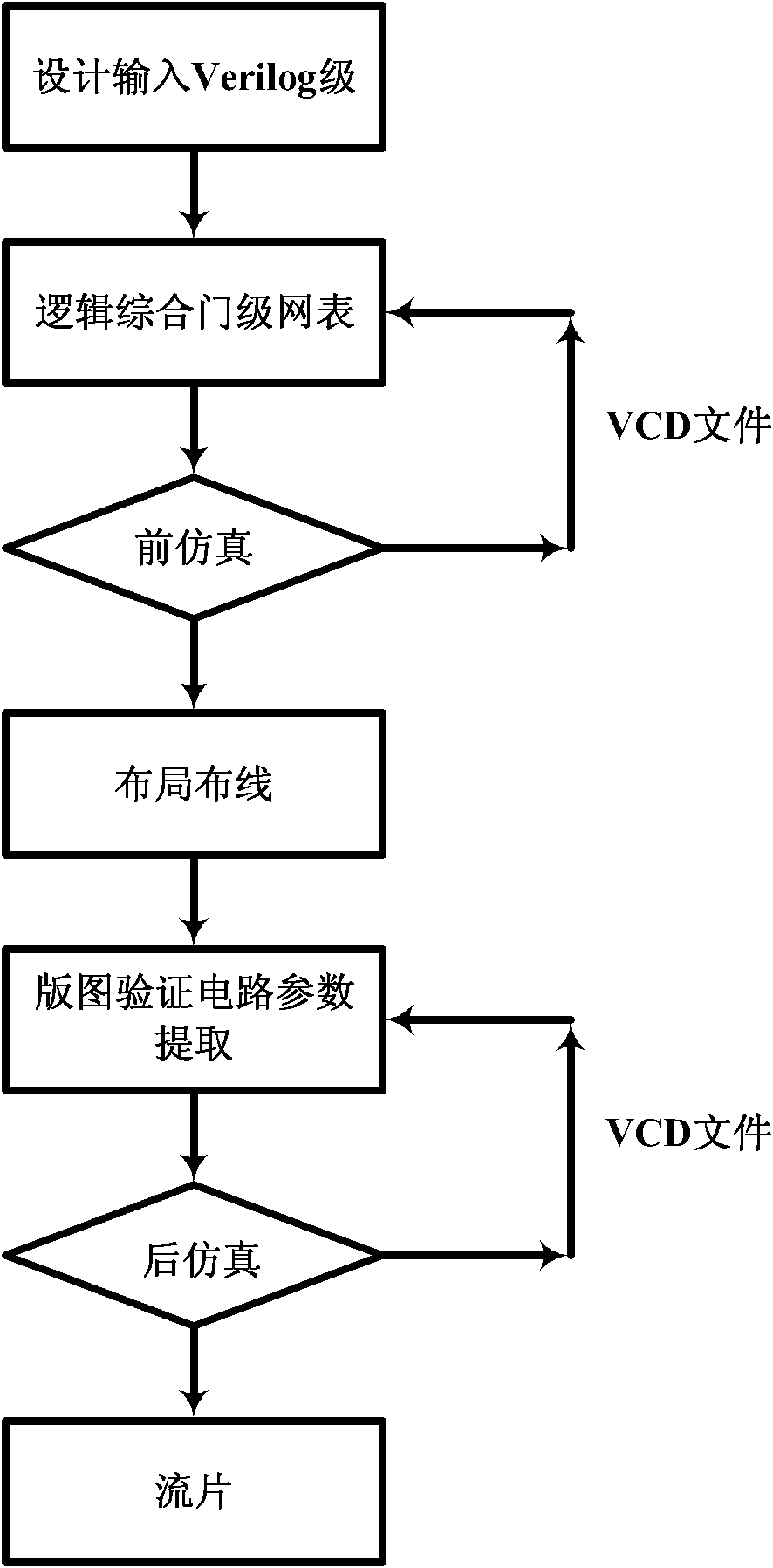
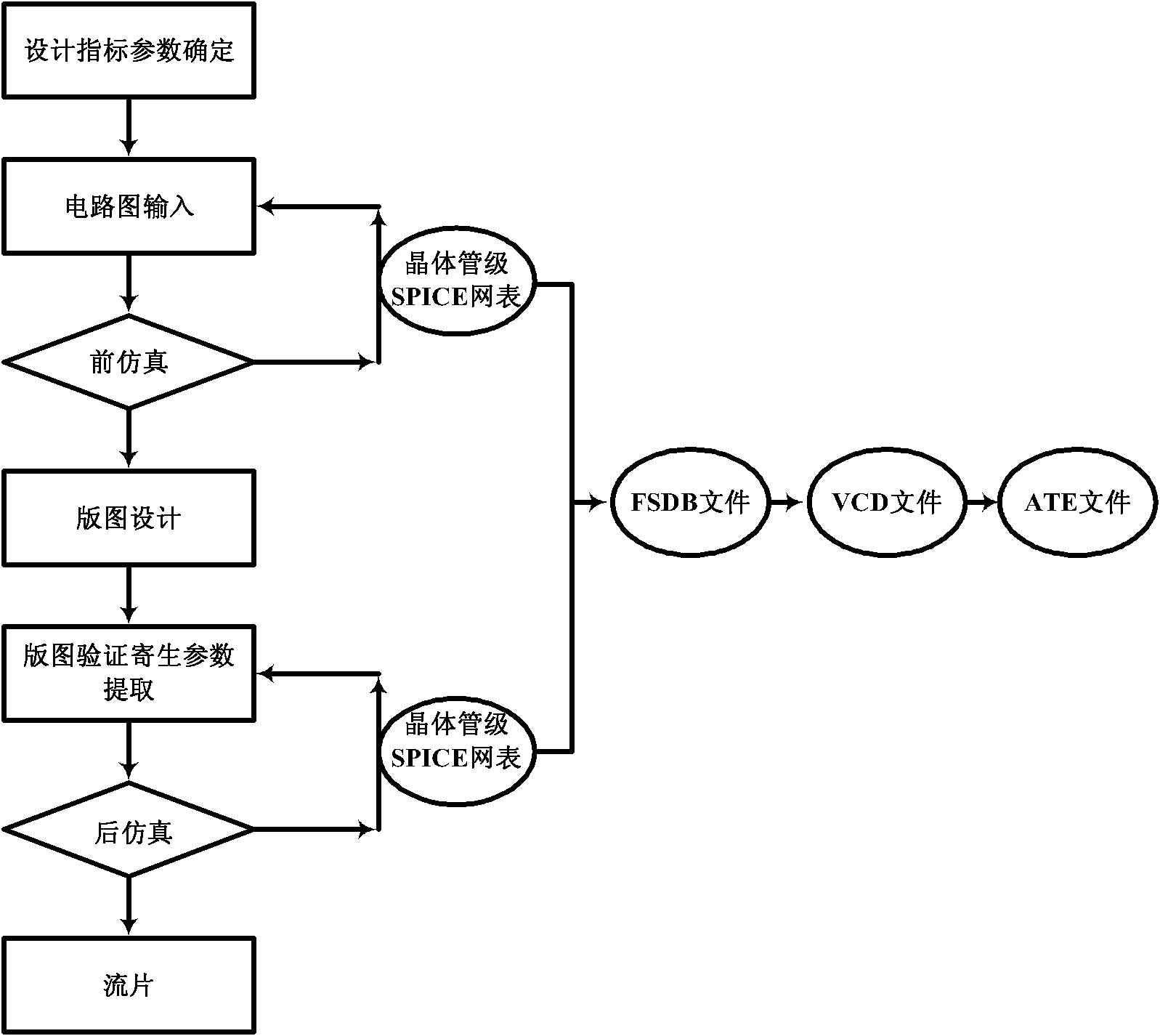
[0019] The features and technical effects of the technical solution of the present invention will be described in detail below with reference to the accompanying drawings and in combination with schematic embodiments, and a test design method for an analog and digital-analog hybrid chip is disclosed. It should be pointed out that similar reference numerals represent similar structures, and the terms "first", "second", "upper", "lower" and the like used in this application can be used to modify various device structures or process steps . These modifications do not imply spatial, sequential or hierarchical relationships of the modified device structures or process steps unless otherwise specified.

[0020] Refer to the attached Figure II As shown, the design and testing process of the analog integrated circuit used in the present invention will be described in detail. In the analog circuit design part, it is the same as the general analog circuit design. The process is from ...


PUM


Abstract

The invention provides an integrated circuit testing method, which comprises the steps of design index parameter determination, circuit diagram input, pre-simulation, layout design, layout verification and parasitic parameter extraction, post-simulation and tape-out. The integrated circuit testing method is characterized in that both the pre-simulation and the post-simulation use a transistor-level SPICE netlist, which can be converted to documents required for an automatic testing platform. The testing method provided by the invention can be used to greatly shorten the original test vector writing time for chip testing personnel, speed up the progress of the test, avoid understanding deviation between designers and testers and achieve seamless butting.

Description

technical field [0001] The invention relates to an integrated circuit testing method, in particular to an analog and digital-analog hybrid integrated circuit test. Background technique [0002] Nowadays, with the continuous improvement of chip design level and the improvement of processing technology, the number of pins of a single chip is increasing, and the functions are becoming more and more complex. This poses a new problem for test engineers: facing such a chip with complex functions, how can we write a comprehensive and effective test pattern file that basically covers most of the functions of the chip? Moreover, after the writing is completed, the entry of the file will also be a cumbersome task. Therefore, there is an urgent need for methods to flexibly convert between electronic design automation (EDA) tools and automatic test equipment (ATE) platforms. [0003] VCD file is the abbreviation of Value Change Dump (Value Change Dump), which is the standard output fo...

Claims


Application Information

Patent Timeline
Patent Type & Authority Applications(China)
IPC IPC(8): G01R31/3167
Inventor 郝乐宿晓慧韩郑生罗家俊
Owner INST OF MICROELECTRONICS CHINESE ACAD OF SCI
Why Eureka
Try Eureka