Gain embedded dynamic random access memory (eDRAM) unit structure
A technology of memory cells and MOS tubes, applied in the field of memory, can solve the problems of high refresh frequency, serious leakage, and aggravated tunneling effect.
- Summary
- Abstract
- Description
- Claims
- Application Information
AI Technical Summary
Problems solved by technology
Method used
Image


Examples
Embodiment Construction
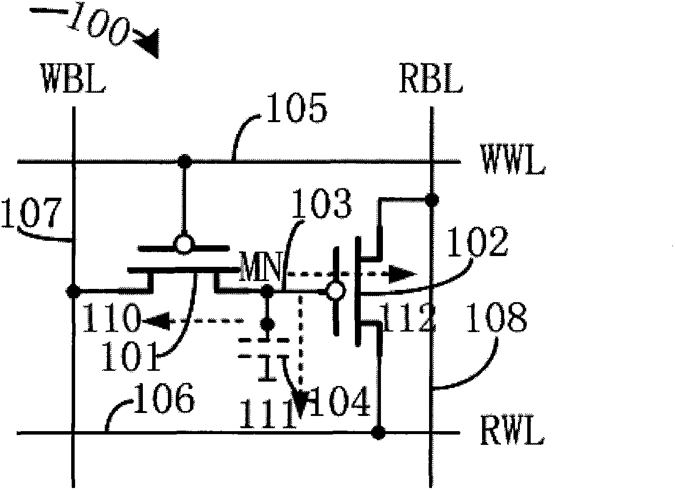
[0023] Referring to FIG. 3 , it is a layout and a cross-sectional view of a memory cell according to an embodiment of the present invention. The eDRAM unit 300 of this embodiment is also figure 1 The structure shown includes a write MOS transistor, a read MOS transistor, a write word line, a write bit line, a read word line, and a read word line. Therefore, the schematic circuit structure of the eDRAM unit 300 is the same as figure 1 The schematic diagram of the circuit structure of the eDRAM unit shown is the same, and the connection relationship between the write MOS transistor, the read MOS transistor, the write word line, the write bit line, the read word line and the read word line, and the functions realized are also the same, and will not be repeated here. For repeat.
[0024] Specifically, 301 represents the source region of the write MOS transistor 101, 302 represents the gate of the write MOS transistor, 305 represents the active region of the read MOS transistor 10...
PUM
 Abstract
Description
Claims
Application Information
 - R&D
- Intellectual Property
- Life Sciences
- Materials
- Tech Scout
- Unparalleled Data Quality
- Higher Quality Content
- 60% Fewer Hallucinations
Browse by: Latest US Patents, China's latest patents, Technical Efficacy Thesaurus, Application Domain, Technology Topic, Popular Technical Reports.
© 2025 PatSnap. All rights reserved.Legal|Privacy policy|Modern Slavery Act Transparency Statement|Sitemap|About US| Contact US: help@patsnap.com