Method for processing orientation-deflected seed crystals

A processing method and crystal orientation technology, which is applied in the field of monocrystalline silicon single crystal seed crystal production, can solve problems such as inapplicability and difficulty in achieving precise control, so as to increase output, improve alignment accuracy, and reduce deviation distance Effect

Active Publication Date: 2013-01-16
ZHEJIANG COWIN ELECTRONICS
View PDF5 Cites 13 Cited by
  • Summary
  • Abstract
  • Description
  • Claims
  • Application Information

AI Technical Summary

Problems solved by technology

[0007] Patent CN 101537666A "Processing Method of Large Off-Angle Seed Crystal" mainly describes a method for processing high-off-angle seed crystals used in gallium arsenide. This method is suitable for large deflection angles. ~22°, it is difficult to achieve precise control, and this method is applicable to GaAs single crystal, which is a compound element single crystal, and there is still a certain difference in crystal orientation between silicon single crystal and single element single crystal, so it cannot be applied

Method used


Image

  • Method for processing orientation-deflected seed crystals
  • Method for processing orientation-deflected seed crystals
  • Method for processing orientation-deflected seed crystals

Examples


Embodiment 1

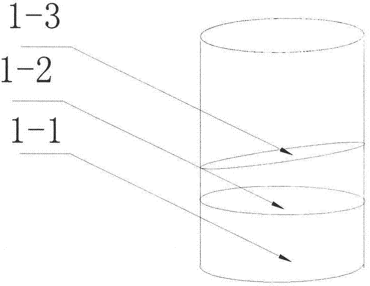
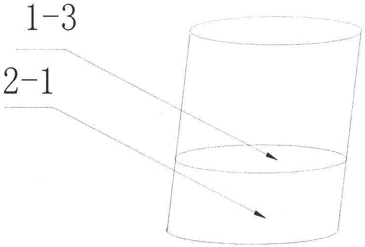
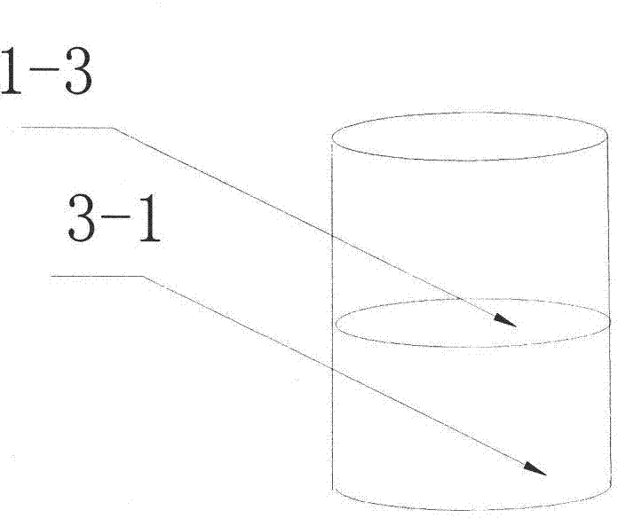
[0046] N-type silicon single crystal 4-inch silicon wafers with a partial crystal orientation of 4° are used for the production and processing of orthocrystalline seed crystals and partial crystal orientation seed crystals of 3° respectively.

[0047] 1. Single crystal growth: use 2 sets of CG-3000 single crystal furnaces, 14-inch thermal field growth, grow 4-inch silicon single crystals respectively, and feed 25kg.

[0048] 2. Carry out single crystal growth according to the process of charging, heating, chemical material, seeding, seeding, shouldering, shoulder turning, equal diameter and finishing process, and obtain one orthocrystalline ingot and one crystal ingot with monomorphic orientation.

[0049] 3. Carry out single crystal cutting according to the requirements of resistivity, cut 300mm long crystal ingots from each crystal ingot, and carry out wire cutting and glue according to the partial crystal direction of 4°, and use the same multi-wire cutting machine to cut a...


PUM


Abstract

The invention discloses a method for processing orientation-deflected seed crystals. The method includes selecting crystal ingots meeting specific requirements and determining directions of main reference planes according to growth edge lines; performing primary rounding processing by a rounder; precisely positioning the main reference planes by an X-ray orientation diffraction instrument and finding OF planes of orientation deflection; performing adjusted orientation deflection cutting for an end surface of each crystal ingot by an internal dicing saw to meet specified requirements on the orientation deflection and parallelly cutting another end surface of the crystal ingot; performing secondary rounding processing according to the orientation-deflected end surfaces; perpendicularly extracting seed crystals from the processed crystal ingots by a milling machine and a seed crystal extracting device; performing clamped surface processing, chemical polishing and cleaning for the extracted seed crystals to obtain the orientation-deflected seed crystals. By using the orientation-deflected seed crystals processed by the method for producing orientation-deflected silicon wafers, the processing yield can be effectively increased, the yield of the wafers from crystal bars in unit weight can be effectively increased, and the silicon wafer chamfering processing efficiency can be effectively improved.

Description

technical field [0001] The invention belongs to the field of semiconductor silicon single crystal growth, and in particular relates to a method for making a silicon single crystal monocrystal orientation seed crystal, which can realize precise crystal orientation deviation and meet the production and processing requirements of epitaxial substrate silicon wafers and other silicon wafers with partial crystal orientation requirements. Demand, can reduce production loss, improve film output rate, and reduce processing volume. Background technique [0002] For semiconductor silicon wafers, according to the different surface processing methods and the extension degree of the pre-device manufacturing process, it can be divided into cutting wafers, grinding wafers, polishing wafers, and epitaxial wafers. According to the crystal orientation, there are mainly <111>, <100>, <110> crystal orientations, among which <111>, <100> crystal orientations are the ...

Claims


Application Information

Patent Timeline
Patent Type & Authority Applications(China)
IPC IPC(8): B28D5/00B28D7/04
Inventor 孙新利
Owner ZHEJIANG COWIN ELECTRONICS
Why Eureka
Try Eureka