
A light-emitting diode chip and its manufacturing method

A technology of light-emitting diodes and manufacturing methods, which is applied in the direction of semiconductor devices, electrical components, circuits, etc., can solve the problems of many times of photolithography, achieve the effect of simplifying the process steps, increasing the area of ​​the light-emitting area, and saving the number of times of photolithography

Active Publication Date: 2019-10-29
XIANGNENG HUALEI OPTOELECTRONICS
View PDF4 Cites 0 Cited by
  • Summary
  • Abstract
  • Description
  • Claims
  • Application Information

AI Technical Summary

Problems solved by technology

[0005] The purpose of the present invention is to provide a method for manufacturing a light-emitting diode chip to solve the technical problem of too many times of photolithography in the opening process

Method used


Image

  • A light-emitting diode chip and its manufacturing method
  • A light-emitting diode chip and its manufacturing method
  • A light-emitting diode chip and its manufacturing method

Examples


Embodiment Construction

[0026] The embodiments of the present invention will be described in detail below with reference to the accompanying drawings, but the present invention can be implemented in various ways defined and covered by the claims.

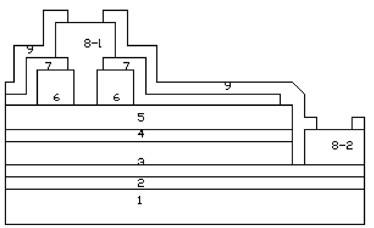
[0027] see figure 1 , figure 2 , the application provides a simpler manufacturing method, which specifically includes the following steps:

[0028] Step 1: disposing the buffer layer on the substrate along the axial direction, disposing the N-type semiconductor layer on the buffer layer; disposing the light-emitting layer on the N-type semiconductor layer, disposing the P-type semiconductor layer on the light-emitting layer;

[0029] Step 2: Deposit the current blocking layer on the upper part of the chip body by plasma enhanced chemical vapor deposition, and make the required pattern by photolithography. At this time, the current blocking layer under the P electrode is not open. see figure 2 (a) and figure 2 (b).

[0030] Step 3: The transparent ...


PUM


Abstract

The invention provides a light-emitting diode chip and a manufacturing method thereof. The manufacturing method comprises the following steps: A, depositing a current baffle layer on a P-type semiconductor layer, wherein the thickness of the current baffle layer is 250-1000nm, and no hole is formed in the current baffle layer at the moment; B, depositing a transparent conductive layer on the current baffle layer without holes, wherein no hole is formed in the current baffle layer, but holes are formed in the transparent conductive layer; performing wet-method corrosion, and retaining a photoresist; C, performing dry-method etching on the current baffle layer till the upper surface of a P-type gallium nitride layer. The manufacturing method provided by the invention is simple in step, easy in process parameter control and applicable to industrial production.

Description

technical field [0001] The invention relates to the technical field of semiconductors, in particular to a light emitting diode chip and a manufacturing method thereof. Background technique [0002] Since the adhesion between metal and ITO and the adhesion between metal and silicon oxide cannot meet the push-pull force requirements when packaging and bonding wires, it will cause the electrodes to fall off, causing fatal defects in semiconductor devices. [0003] In order to solve the above problems, all LED chips on the market need openings in the current blocking layer and the ITO blocking layer under the P electrodes. The usual practice is as figure 1 As shown, it is divided into five photolithography, namely: current blocking layer photolithography (holes under the P electrode), transparent conductive layer photolithography (holes under the P electrode), mesa etching photolithography, NP electrode photolithography, Protective layer photolithography. If this is done, the...

Claims


Application Information

Patent Timeline
Patent Type & Authority Patents(China)
IPC IPC(8): H01L33/00H01L33/14
CPCH01L33/0075H01L33/145
Inventor 何鹏
Owner XIANGNENG HUALEI OPTOELECTRONICS
Learn More