Shift register circuit and chip

A technology of shift registers and circuits, which is applied in the electronic field to achieve the effects of programmable performance, low power consumption, and high storage density

CN102881333AActive Publication Date: 2013-01-16PEKING UNIV
3 Cites 5 Cited by

Patent Information

Authority / Receiving Office
CN · China
Patent Type
Applications(China)
Current Assignee / Owner
Publication Date
2013-01-16

Smart Images

  • Figure 1
    Figure 1
  • Figure 2
    Figure 2
  • Figure 3
    Figure 3
Patent Text Reader

Abstract

The embodiment of the invention discloses a shift register circuit and a chip. The circuit comprises a resistance changing memristor matrix and a current sensitive module, wherein positive phase input ends of the same column of resistance changing memristors in the resistance changing memristor matrix are connected, so that the positive phase input ends of the same column of resistance changing memristors are served as signal input ports; negative phase input ends of the same column of resistance changing memristors in the resistance changing memristor matrix are connected with the input end of the current sensitive module, so that the output end of the current sensitive module is served as a signal output port; the input end of the current sensitive module is connected to low electric level during operation; when the current received by the input end of the current sensitive module is more than threshold current, the output end of the current sensitive module outputs high electric level; and when the current received by the input end of the current sensitive module is less than the threshold current, the output end of the current sensitive module outputs low electric level. In the embodiment of the invention, the occupied area of the shift register circuit is saved and the programmable performance of the shift register circuit is achieved.
Need to check novelty before this filing date? Find Prior Art

Description

technical field

[0001] The invention relates to the field of electronic technology, in particular to a shift register circuit and a chip. Background technique

[0002] Shift register circuits are usually based on metal-oxide-semiconductor (MOS, Metal-Oxide-Semiconductor) tube storage devices. As the requirements for chip integration become higher and higher, the size of shift register circuits is also decreasing, but Due to the limitation of the size of the MOS transistor storage device itself, the shift register circuit in the prior art has a technology node with the smallest size. Contents of the invention

[0003] Embodiments of the present invention provide a shift register circuit and a chip, which are used to solve the problem that the shift register circuit in the prior art has a minimum size technology node.

[0004] In order to solve the above problems, the embodiment of the present invention discloses the following technical solutions:

[0005] On the one hand,...

Examples

Embodiment Construction

[0024] The technical solutions in the embodiments of the present invention will be clearly and completely described below in conjunction with the accompanying drawings in the embodiments of the present invention. Obviously, the described embodiments are only some, not all, embodiments of the present invention. Based on the embodiments of the present invention, all other embodiments obtained by persons of ordinary skill in the art without creative efforts fall within the protection scope of the present invention.

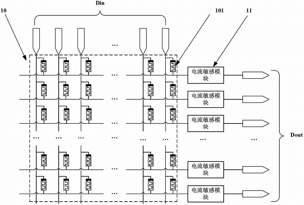
[0025] Such as figure 1 Shown is a schematic diagram of a shift register circuit in an embodiment of the present invention.

[0026] The shift register circuit may include a resistive memristor matrix 10 and a current sensing module 11 . In the resistive memristor square matrix 10, the positive phase input terminals of the same column resistance variable memristor 101 are connected, so that the positive phase input terminal of the same column resistance variable mem...