Light-emitting diode (LED) light source module

A technology of LED light source and LED chip, applied in the direction of light source, electric light source, point light source, etc., can solve the problems of inconsistent light attenuation speed of chips, undesired LED light source, and need to open mold for heat dissipation fins, so as to achieve light weight and structure. Simple and reasonable, the effect of improving the light output rate

Active Publication Date: 2013-01-23
广东宏泰智慧城市科技有限公司
View PDF4 Cites 5 Cited by
  • Summary
  • Abstract
  • Description
  • Claims
  • Application Information

AI Technical Summary

Problems solved by technology

For LED chips, if the heat is concentrated inside the chip and cannot be effectively diffused to the surrounding environment, the reliability of the device
For LED light source modules, if the temperature of different chips is inconsistent, it may lead to inconsistent light attenuation speeds of different chips.
At present, heat dissipation fins are used on the circuit board to dissipate heat. Although this method can achieve a better heat dissipation effect, the disadvantages are as follows: 1) The weight increases, which is not advisable for LED light sources; 2) Heat dissipation fins The chip needs to be molded, which increases the cost

Method used


Image

  • Light-emitting diode (LED) light source module
  • Light-emitting diode (LED) light source module
  • Light-emitting diode (LED) light source module

Examples


specific Embodiment 1

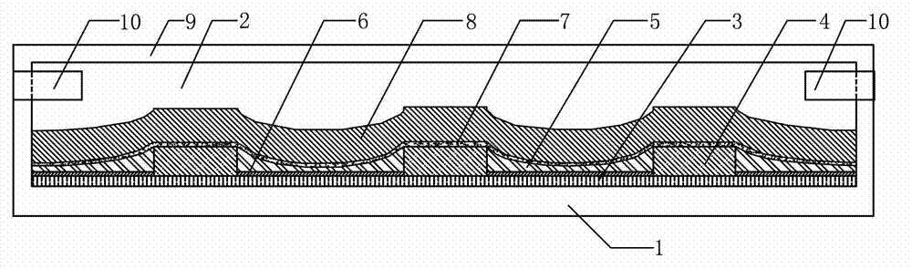
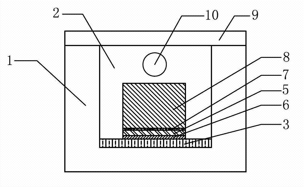
[0025] Figure 1-Figure 3 Embodiment 1 of the present invention is constituted.

[0026] refer to figure 1 and figure 2 , this embodiment includes a substrate 1, a groove 2 opened on the substrate 1, and a conductive layer 3 packaged in the groove 2, and three LED chips 4 and four photosensitive units 5 are installed on the conductive layer 3, so The LED chips 4 and the photosensitive units 5 are alternately arranged; an insulating layer 6 is arranged between each photosensitive unit 5 and the conductive layer 3, and a reflective layer 7 and The heat dissipation layer 8 , a circuit for electrically connecting the LED chips 4 is arranged on the bottom of the groove 2 .

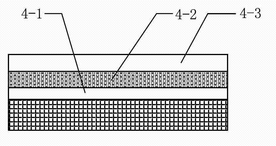
[0027] refer to image 3 , the LED chip 4 is sequentially coated with a first silica gel layer 4-1, a fluorescent layer 4-2 and a second silica gel layer 4-3 from the light-emitting surface, and the second silica gel layer 4-3 is in the shape of a film.

[0028] In this embodiment, a transparent material ...

specific Embodiment 2

[0034] The main features of this embodiment are: the transparent material layer 9 is made of glass, and the second silica gel layer 4-3 of the LED chip 4 is in the shape of a convex lens or a microlens array. All the other are with specific embodiment 1.

specific Embodiment 3

[0035] The main feature of this embodiment is that four or more LED chips 4 and five or more photosensitive units 5 are mounted on the conductive layer 3 . All the other are with specific embodiment 1.


PUM


Abstract

The invention discloses a light-emitting diode (LED) light source module, which comprises a substrate (1), a groove (2) and a conductive layer (3), wherein the groove (2) is formed in the substrate (1); the conductive layer (3) is packaged in the groove (2) and is provided with a plurality of LED chips (4) and a plurality of photosensitive units (5); the thicknesses of the photosensitive units (5) are smaller than those of the LED chips (4); the LED chips (4) and the photosensitive units (5) are arranged in a staggered manner; an insulating layer (6) is arranged between each photosensitive unit (5) and the corresponding conductive layer (3); a reflecting layer (7) is arranged on the upper surface of each LED chip (4); a radiating layer (8) is arranged on the upper surface of each photosensitive unit (5); and circuits by which the LED chips (4) are electrically connected with one another are distributed at the bottom of the groove (2). By the LED light source module, the radiating capacity of the whole module is greatly improved, heat among the LED chips is dissipated uniformly, the service lives of the LED chips are prolonged, and a phenomenon that a large amount of hot air spreads to air at one time can be avoided.

Description

technical field [0001] The invention relates to an LED light source module, in particular to an LED light source module integrated with a plurality of LED chips. The invention belongs to the technical field of LED light source integration. Background technique [0002] A light emitting diode (Light Emitting Diode, hereinafter referred to as LED) is a semiconductor electronic component that can emit light, which can directly convert electricity into light. The main body of the LED is a semiconductor wafer, which consists of two parts, one is a P-type semiconductor, which is dominated by holes, and the other is an N-type semiconductor, which is mainly electrons. The two semiconductors are connected to form A P-N junction; adding a specific compound at the P-N junction can emit light of a specific color, such as a gallium arsenide phosphor diode emits red light, a gallium phosphide diode emits green light, and a silicon carbide diode emits yellow light. [0003] With the cont...

Claims


Application Information

Patent Timeline
Patent Type & Authority Applications(China)
IPC IPC(8): F21S2/00F21V29/00F21V19/00F21V17/00F21Y101/02F21K9/66F21K9/68F21V29/508F21V29/74F21Y115/10
Inventor 吴飞
Owner 广东宏泰智慧城市科技有限公司
Why Eureka
Try Eureka