High-power semiconductor laser with non-absorbing windows

A non-absorbing, laser technology, applied in the structure of optical waveguide semiconductors, the structure of active regions, etc., can solve the problems of reducing the output power of lasers, achieve simple and easy manufacturing process, increase output power, and increase optical catastrophe damage threshold Effect

Active Publication Date: 2013-01-23
XIAN UNIV OF TECH
View PDF3 Cites 11 Cited by
  • Summary
  • Abstract
  • Description
  • Claims
  • Application Information

AI Technical Summary

Problems solved by technology

[0005] The purpose of the present invention is to provide a high-power semiconductor laser with a non-absorbing window, which solves the problem that in the prior art, due to the relatively uniform distribution of the absorption energy levels of the impurities introduced when the quantum wells are mixed, it will cause extra light outside the central area of ​​the spot. absorption, thereby reducing the output power of the laser

Method used


Image

  • High-power semiconductor laser with non-absorbing windows
  • High-power semiconductor laser with non-absorbing windows

Examples


Embodiment 1

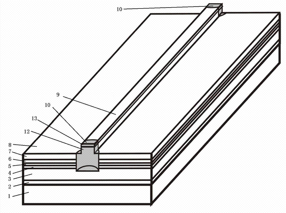
[0017] refer to figure 1 , is a schematic structural diagram of a high-power semiconductor laser with a 670nm non-absorbing window in Example 1 of the present invention. The non-absorbing window 10 is distributed on the upper surface of the epitaxial wafer structure of the laser. 1. Epitaxially grown buffer layer 2, lower confinement layer 3, lower waveguide layer 4, quantum well and quantum barrier region 5, upper waveguide layer 6, upper confinement layer 7 and upper contact layer 8, longitudinal centerline of upper contact layer 8 A ridge waveguide 9 and a semi-cylindrical non-absorbing window 10 are arranged on it, the non-absorbing window 10 includes a semi-cylindrical planar portion 12 and a semi-cylindrical arc portion 13, the planar portion 12 is used to serve as the light-emitting surface of the laser, The arc portion 13 is used as the interface between the non-absorbing area and the normal area; the central area of ​​the non-absorbing window 10 coincides with the cen...

Embodiment 2

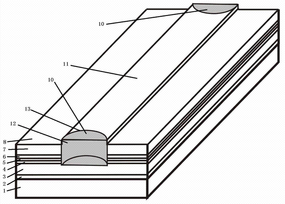
[0023] refer to figure 2 , is a schematic diagram of the structure of the 808nm non-absorbing window high-power semiconductor laser in Example 2 of the present invention. The difference from Example 1 is that the laser in Example 2 is a strip structure, and the width of the strip area is 60 microns. The non-absorbing window 10 is distributed on the surface of the laser epitaxial wafer structure, and the described epitaxial wafer structure is sequentially provided with a substrate 1, an epitaxially grown buffer layer 2, a lower confinement layer 3, a lower waveguide layer 4, a quantum well and The quantum barrier region 5, the upper waveguide layer 6, the upper confinement layer 7 and the upper contact layer 8, the longitudinal center line of the upper contact layer 8 are provided with a strip region 11 and a non-absorbing window 10, and the non-absorbing window 10 includes a semi-cylindrical Planar portion 12 and semi-cylindrical arc portion 13, semi-cylindrical planar portio...


PUM


Abstract

The invention discloses a high-power semiconductor laser with non-absorbing windows, wherein the non-absorbing windows are positioned above a ridge-shaped or bar-shaped part of the laser and distributed at two ends of a laser cavity surface and distributed in a semicolumnar shape, the planar part of each non-absorbing window is a light emergent cavity surface of the laser, and the arc-surface part of each non-absorbing window is positioned inside the cavity length of the laser; the depth of each non-absorbing window should exceed that of an upper waveguide layer of an active area of the laser; in the ridge-shaped waveguide structure, the diameter of the non-absorbing window is larger than or equal to 1 micrometer and smaller than 20 micrometers; or in the bar-shaped laser structure, the diameter of each non-absorbing window is larger than 3 micrometers and smaller than 900 micrometers. According to the high-power semiconductor laser, the optical catastrophe damage threshold is greatly increased, the light absorption caused by impurity level is effectively reduced, and the maximum output power of the laser is promoted; and the high-power semiconductor laser is simple in process and feasible and has a large-scale production feature.

Description

technical field [0001] The invention belongs to the technical field of semiconductor laser equipment and relates to a high-power semiconductor laser with a non-absorption window. Background technique [0002] Semiconductor lasers have become one of the most important semiconductor optoelectronic devices due to their wide range of wavelength selection, small size, low power consumption, high efficiency, good inheritance, and low cost. Among them, high-power semiconductor lasers are widely used in laser storage, laser display, laser printing, material processing, laser marking, biomedicine, medical equipment, space optical communication and other fields. Guidance, laser night vision, laser radar, laser fuze, laser weapons, war simulation, etc. High-power semiconductor laser technology covers almost all fields of optoelectronics. The development of high-performance high-power lasers requires coordination and cooperation in many aspects such as laser epitaxial wafer structure d...

Claims


Application Information

Patent Timeline
Patent Type & Authority Applications(China)
IPC IPC(8): H01S5/22H01S5/34
Inventor 林涛张浩卿马新尖李超林楠
Owner XIAN UNIV OF TECH
Why Eureka
Try Eureka