
Semiconductor laser manufactured by mixed zinc oxide quantum well and manufacturing method of semiconductor laser

A technology of quantum well hybridization and fabrication method is applied in the field of laser fabrication to achieve the effect of improving the light field mode, the fabrication process is simple and feasible, and the compatibility is good.

Active Publication Date: 2015-07-01
XIAN UNIV OF TECH
View PDF6 Cites 9 Cited by
  • Summary
  • Abstract
  • Description
  • Claims
  • Application Information

AI Technical Summary

Problems solved by technology

[0007] The purpose of the present invention is to provide a semiconductor laser made by zinc oxide quantum well hybridization, which solves the problem of optical limitation on the side of the light-emitting region and leakage current outside the light-emitting region after the non-absorbing window is made by quantum well hybridization technology in the prior art.

Method used


Image

  • Semiconductor laser manufactured by mixed zinc oxide quantum well and manufacturing method of semiconductor laser

Examples


Embodiment 1

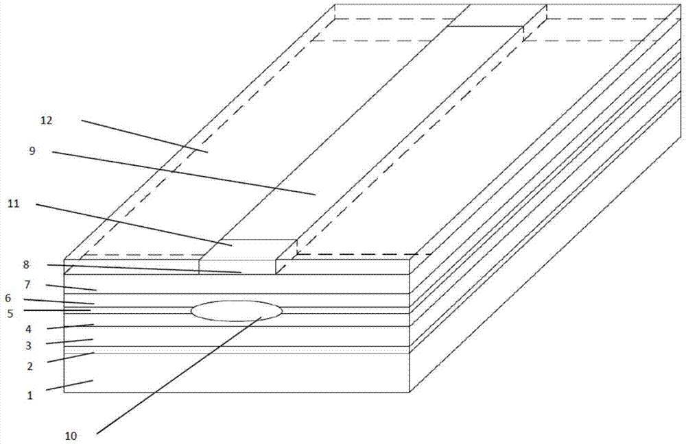
[0044] Embodiment 1 is the 808nm strip structure high-power semiconductor laser that utilizes zinc oxide quantum well hybridization to make, and its structure is as follows figure 1 As shown, including the epitaxial wafer, the specific structure of the epitaxial wafer is arranged in order from bottom to top: substrate 1, buffer layer 2, lower confinement layer 3, lower waveguide layer 4, quantum well and quantum barrier region 5, upper waveguide layer 6 , the upper confinement layer 7 and the upper ohmic contact layer 8 . The longitudinal centerline of the upper ohmic contact layer 8 is provided with a strip-shaped light-emitting area 9, and the strip-shaped light-emitting area 9 is surrounded by a zinc oxide film layer grown after the upper ohmic contact layer 8 is corroded. The thickness of the zinc oxide film layer is the same as that of the upper ohmic contact layer. The thicknesses of the layers 8 are equal, and the zinc oxide film layer is divided into a zinc oxide film ...


PUM


Abstract

The invention discloses a semiconductor laser manufactured by mixed zinc oxide quantum well and a manufacturing method of the semiconductor laser. The semiconductor laser comprises an epitaxial wafer; a strip-shaped lighting area is formed in the epitaxial wafer; an zinc oxide film layer develops on the upper surface of the epitaxial wafer and is divided into two parts, wherein the first part is used for inducing zinc oxide quantum well to mix and then forming non-absorbing windows in light outgoing cavity surfaces at two ends of the laser; the depth of the non-absorbing windows exceeds that of an active source in the epitaxial wafer; the second part is used for inducing zinc oxide quantum well to mix and then forming refraction rate light waveguide areas in two ends of the strip-shaped lighting area of the laser. The invention further discloses a manufacturing method of the semiconductor laser. With the adoption of the semiconductor laser, the problem that the side surface optical limitation and external electricity leakage of the lighting area cannot be avoided after manufacturing the non-absorbing windows by the quantum well mixing technology in the prior art can be solved.

Description

technical field [0001] The invention belongs to the technical field of semiconductor laser equipment, and in particular relates to a semiconductor laser produced by zinc oxide quantum well hybridization, and also relates to a manufacturing method of the laser. Background technique [0002] Semiconductor lasers have become one of the most important semiconductor optoelectronic devices due to their wide range of wavelength selection, small size, low power consumption, high efficiency, good inheritance, and low cost. Among them, high-power semiconductor lasers are widely used in laser storage, laser display, laser printing, material processing, laser marking, biomedicine, medical equipment, space optical communication and other fields. At the same time, they can also be used in laser targeting and laser guidance in the military field. , laser night vision, laser radar, laser fuze, laser weapons, war simulation, etc. High-power semiconductor laser technology covers almost all f...

Claims


Application Information

Patent Timeline
Patent Type & Authority Applications(China)
IPC IPC(8): H01S5/34
Inventor 林涛张浩卿孙航郭恩民孙锐娟
Owner XIAN UNIV OF TECH
Learn More