Display element, display, and projection display device

一种显示元件、发光元件的技术,应用在电气元件、光学元件、利用投影装置图像重现器等方向,达到高方向性、高亮度和的效果

Inactive Publication Date: 2013-01-23
NEC CORP
View PDF6 Cites 8 Cited by
  • Summary
  • Abstract
  • Description
  • Claims
  • Application Information

AI Technical Summary

Problems solved by technology

[0004] Furthermore, as described in Non-Patent Document 1, such a projector with a solid-state light source is limited by etendue, which depends on the product of the area of ​​the light source and the emission angle

Method used


Image

  • Display element, display, and projection display device
  • Display element, display, and projection display device
  • Display element, display, and projection display device

Examples


no. 1 example

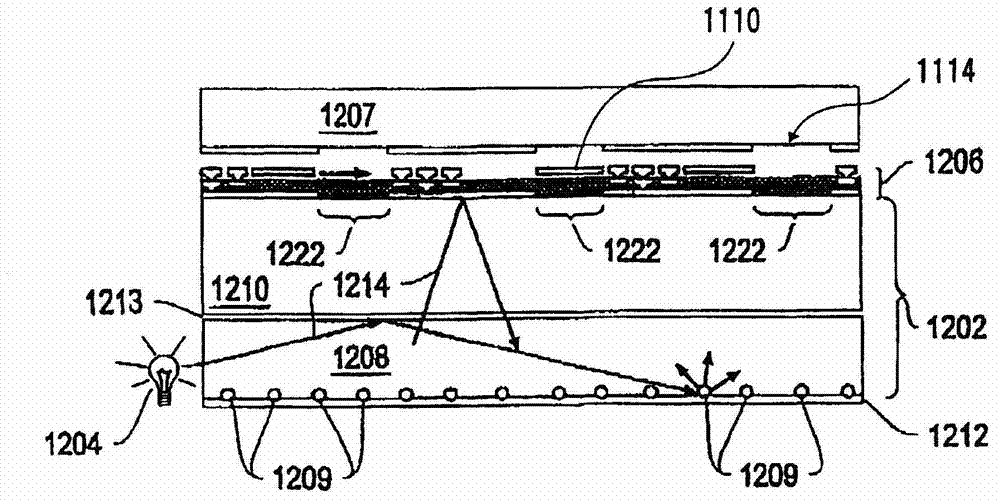
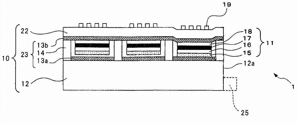
[0051] figure 2 is a sectional view schematically showing the display element according to the first embodiment of the present invention. Since the individual layers of the display element are very thin and their thicknesses vary widely, it is difficult to illustrate the individual layers with exact scale. Accordingly, the drawings do not illustrate the various layers in exact scale, but illustrate them schematically.

[0052] like figure 2 As shown in , the display element 1 according to the present embodiment has a light valve portion 10 including a plurality of optical connection mechanisms 23 as switches for switching between a transmission state and a blocking state of light emitted from a light emitting element 25. a plurality of optical shutter devices; and a substrate 22 through which light from the plurality of optical connection mechanisms 23 passes. Furthermore, display element 1 has a plurality of plasmon coupling sections 11 that cause plasmon coupling to occ...

no. 2 example

[0113] Figure 7 is a sectional view schematically showing a display element according to a second embodiment of the present invention. The display element according to the second embodiment differs from the display element according to the first embodiment in the structure of the optical connection mechanism. Since the structure of the second embodiment is the same as that of the first embodiment except for the optical connection mechanism, structural portions similar to those of the first embodiment are denoted by similar reference numerals, and descriptions thereof will be omitted.

[0114] According to the first embodiment, transparent electrodes 13a and 13b formed in a matrix shape are used. Compared with this, as Figure 7 As shown, the optical connection mechanism 26 of the display element 2 according to the second embodiment has a pair of transparent electrodes 27a and 27b and a TFT 28 that selectively drives the transparent electrode 27b disposed on the substrate 22...

no. 3 example

[0119] Figure 9 is a sectional view schematically showing a display element according to a third embodiment of the present invention. The display element according to the third embodiment differs from the display element according to the first embodiment in the structure of the optical connection mechanism. Since the structure of the third embodiment is the same as that according to the first embodiment except for the optical connection mechanism, structural parts similar to those of the first embodiment are denoted by similar reference numerals, and descriptions thereof will be omitted.

[0120] According to the second embodiment described above, the TFT 28 and the TFT electrodes 29 a and 29 b drive the transparent electrode 27 b arranged on the substrate 22 side. Compared with this, as Figure 9 As shown, the optical connection mechanism 33 of the display element 3 according to the third embodiment has a pair of transparent electrodes 37a and 37b and a TFT 38 that selecti...


PUM

PropertyMeasurementUnit
wavelengthaaaaaaaaaa

Abstract

The present disclosures are provided with: a lightbulb unit (10) that has a substrate (22) that transmits light from a plurality of optical connection mechanisms (23) that switch the transmission and the blocking of light from a light-emitting element (25); and a plasmon coupling unit (11) that generates plasmon coupling by means of light entering from the light-emitting element (25) and that is disposed within the lightbulb unit (10). The plasmon coupling unit (11) has: a carrier generation layer (15) wherein a carrier is generated by means of light entering from the light-emitting element (25); and a plasmon excitation layer (17) that has a higher plasma frequency than the frequency of light arising when exciting the carrier generation layer (15) with the light of the light-emitting element (25). A wavevector conversion layer (19) that converts surface plasmons or light generated by the plasmon excitation layer (17) into light at a predetermined angle of emergence, and then radiates said light is provided on a substrate (22). The plasmon excitation layer (17) is sandwiched between a first dielectric layer (16) and a second dielectric layer (18).

Description

technical field [0001] The present invention relates to a display element, a display device, and a projection display device that emit light using surface plasmons. Background technique [0002] A projector having a solid-state light source using a light-emitting element such as a light-emitting diode (LED) or a semiconductor laser (LD) as a light source has been proposed. A projector with such a solid-state light source has: an illumination optical system into which light emitted from a light-emitting element enters; a light valve having a display element such as a liquid crystal display panel or DMD (Digital Micromirror Device); and a projection optical system that projects light from the light valve to a projection plane. [0003] Projectors with solid-state light sources have the requirement that light loss be minimized in the light path from the light-emitting element to the light valve in order to increase the brightness of the projected image. [0004] Furthermore, ...

Claims


Application Information

Patent Timeline
Patent Type & Authority Applications(China)
IPC IPC(8): G02B26/02G02F1/01B81B3/00G03B21/00G03B21/14
CPCG03B21/00G02B5/008G02B6/0075G02B6/005G02B6/0038G02B26/02G03B21/20G03B21/204G03B21/2066G03B21/28H04N5/74H04N9/3152G03B21/14H04N9/31G03B21/005
Inventor 枣田昌尚今井雅雄富永慎
Owner NEC CORP
Why Eureka
Try Eureka