Method utilizing metal grating to achieve wideband adjustable silicon waveguide optical non-linear four wave mixing enhancement
An optical nonlinear, metal grating technology, applied in nonlinear optics, optics, instruments, etc., can solve the problem that the third-order nonlinear process is not very deep, and achieve the effect of simple structure and easy realization.
- Summary
- Abstract
- Description
- Claims
- Application Information
AI Technical Summary
Problems solved by technology
Method used
Image
Examples
Embodiment 1
[0027] Figure 4 is a plot of the local enhancement factor as a function of grating width.
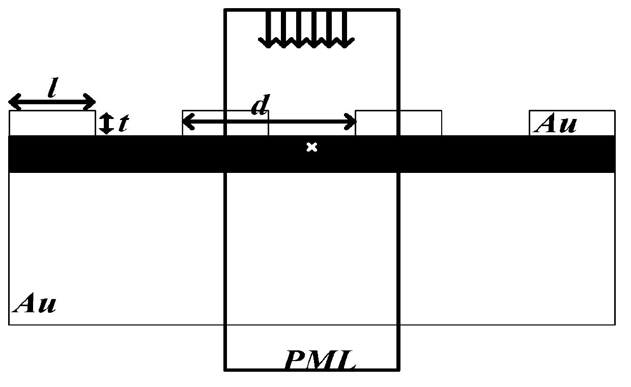
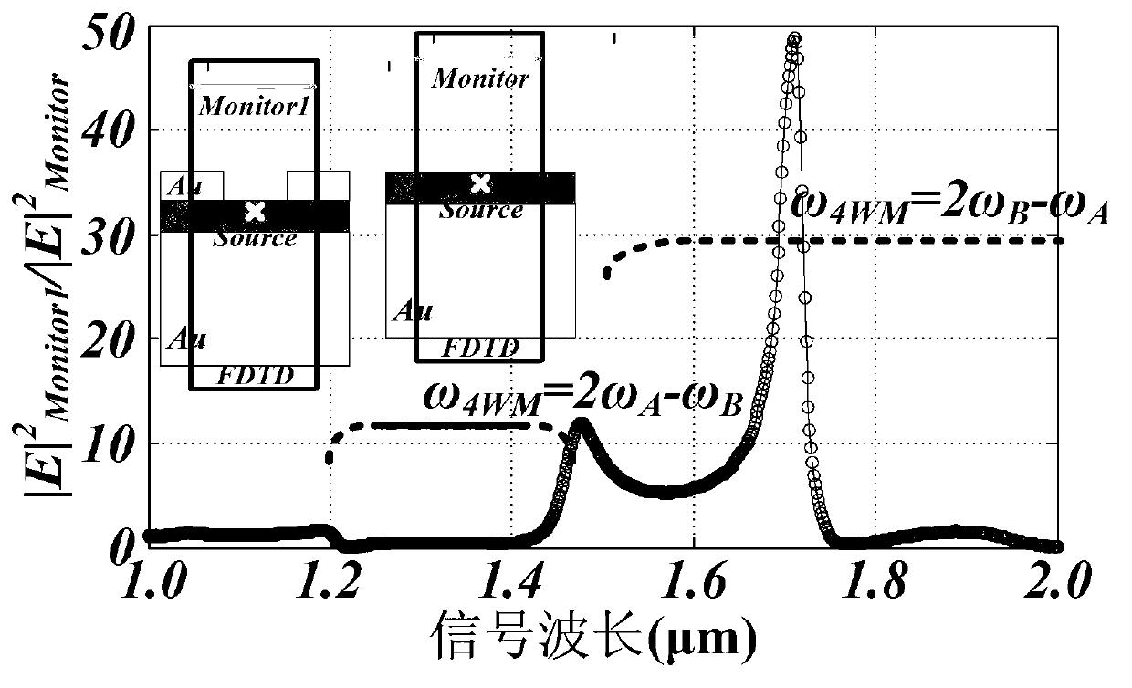
[0028] from image 3 It can be seen that the maximum value of the light intensity enhancement of the four-wave mixing signal is 48.87 at the wavelength λ 4WM =1712nm. In this embodiment, the wavelengths of the two incident lights are selected as λ A =1487nm and λ B =1592nm, the obtained four-wave mixing signal wavelength is λ 4WM =1712nm. The metal thickness is t=50nm, the grating period is d=1000nm, and the silicon thickness is h=100nm.
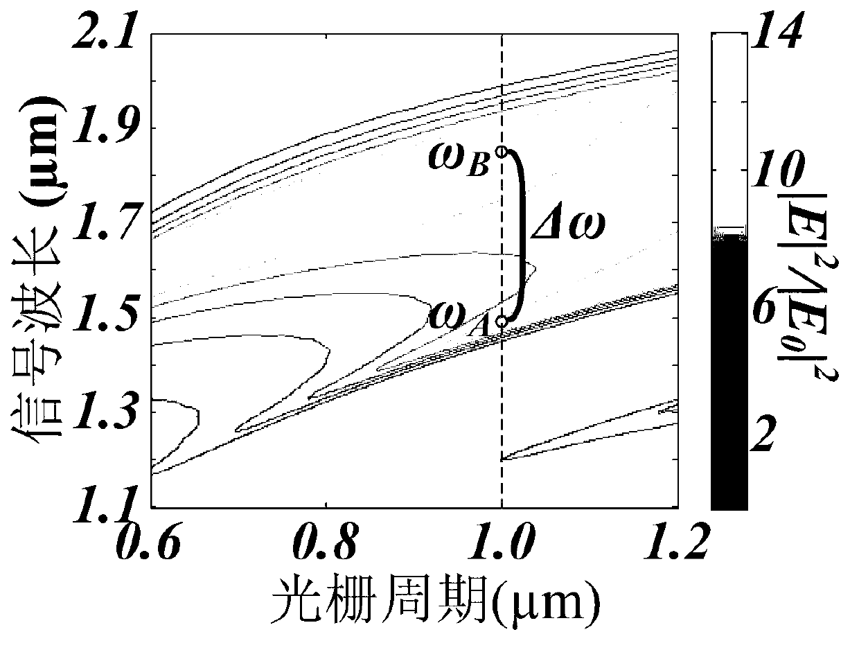
[0029] Calculation method and figure 2 and image 3 same. Increased metal width from 0nm to 1000nm, Figure 4 The change trend of local enhancement factor with grating width is saddle-shaped, and there is a local minimum when the metal width is 347nm(a), 408nm(b), 478nm(c) and 346nm(d). Simultaneous calculation results show that the local enhancement factor (EF) of the four-wave mixing process l When the grating width is 224nm, it can re...
Embodiment 2
[0031] Figure 5 is the local enhancement factor (EF) of the four-wave mixing process l A plot of silicon waveguide thickness as a function of thickness.
[0032] In this embodiment, the wavelengths of the two incident lights are selected as λ A =1487nm and λ B =1592nm, the resulting four-wave mixing wavelength is λ 4WM =1712nm. The metal thickness t=50nm, the metal width l=100nm, the grating period is d=1000nm, and the thickness range h of the silicon waveguide is 60nm-120nm.
[0033] calculation method and figure 2 , image 3 and Figure 4 same. Silicon thickness increased from 60nm to 120nm. Figure 5 It can be seen that the local enhancement factor has a greater enhancement when the thickness of the silicon waveguide is in the range of 90nm-110nm, and the enhancement reaches the maximum when the thickness is 100nm.
PUM
| Property | Measurement | Unit |
|---|---|---|
| thickness | aaaaa | aaaaa |
| width | aaaaa | aaaaa |
| thickness | aaaaa | aaaaa |
Abstract
Description
Claims
Application Information


