Graphene CVD (chemical vapor deposition) direct epitaxial growth method based on sapphire substrate and device fabricated with method

A sapphire substrate, epitaxial growth technology, applied in semiconductor/solid-state device manufacturing, electrical components, circuits, etc., can solve problems such as affecting the electrical properties of graphene devices, difficult to clean and transfer graphene, and reducing graphene mobility, etc. Achieve the effect of improving reliability and electrical characteristics, simplifying growth steps and device manufacturing process steps, and reducing manufacturing costs

Inactive Publication Date: 2013-02-06
XIDIAN UNIV
View PDF0 Cites 9 Cited by
  • Summary
  • Abstract
  • Description
  • Claims
  • Application Information

AI Technical Summary

Problems solved by technology

One of the most significant disadvantages is that a metal catalytic substrate must be used, so it is difficult to cleanly transfer graphene to other dielectric substrates suitable for devices, and residues or contaminants left on graphene after the transfer process will degrade the graphene. Mobility of graphene, thereby affecting the electrical properties of graphene devices

Method used


Image

  • Graphene CVD (chemical vapor deposition) direct epitaxial growth method based on sapphire substrate and device fabricated with method
  • Graphene CVD (chemical vapor deposition) direct epitaxial growth method based on sapphire substrate and device fabricated with method

Examples


Embodiment 1

[0022] The realization steps of the present invention are as follows:

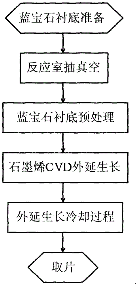
[0023] Step 1, sapphire substrate preparation.

[0024] Put the sapphire substrate into acetone, ethanol and deionized water successively for 10 minutes each time, take out the substrate from the deionized water, and dry it with high-purity nitrogen (99.9999%).

[0025] Step 2, vacuumize the reaction chamber.

[0026] Place the semiconductor device-grade sapphire substrate in the chemical vapor deposition CVD reaction chamber, and pump the vacuum to 10 -6 Torr to remove residual gas in the reaction chamber.

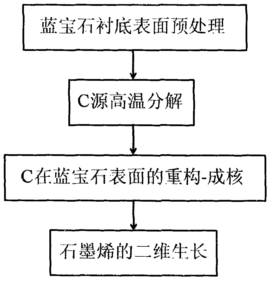
[0027] Step 3, pretreatment of the surface of the sapphire substrate.

[0028] Introduce H into the reaction chamber 2 The substrate surface pretreatment was carried out, the gas flow rate was 2 sccm, the vacuum degree of the reaction chamber was 0.1 Torr, the substrate temperature was 950° C., and the processing time was 5 minutes.

[0029] Step 4, graphene CVD epitaxial growth.

[0030] Introd...

Embodiment 2

[0034] The realization steps of the present invention are as follows:

[0035] Step A, sapphire substrate preparation.

[0036] Put the sapphire substrate into acetone, ethanol and deionized water successively for 10 minutes each time, take out the substrate from the deionized water, and dry it with high-purity nitrogen (99.9999%).

[0037] In step B, the reaction chamber is evacuated.

[0038] Place the semiconductor device-grade sapphire substrate in the chemical vapor deposition CVD reaction chamber, and pump the vacuum to 10 -6 Torr to remove residual gas in the reaction chamber.

[0039] Step C, pretreatment of the surface of the sapphire substrate.

[0040] Introduce H into the reaction chamber 2 The substrate surface pretreatment was carried out, the gas flow rate was 5 sccm, the vacuum degree of the reaction chamber was 0.2 Torr, the substrate temperature was 950° C., and the processing time was 10 minutes.

[0041] Step D, graphene CVD epitaxial growth.

[0042]...

Embodiment 3

[0046] The realization steps of the present invention are as follows:

[0047] Step 1, sapphire substrate preparation.

[0048]Put the sapphire substrate into acetone, ethanol and deionized water successively for 8 minutes each time, take out the substrate from the deionized water, and dry it with high-purity nitrogen (99.9999%).

[0049] Step 2, the reaction chamber is evacuated.

[0050] Place the semiconductor device-grade sapphire substrate in the chemical vapor deposition CVD reaction chamber, and pump the vacuum to 10 -6 Torr to remove residual gas in the reaction chamber.

[0051] Step 3, surface pretreatment of the sapphire substrate.

[0052] Introduce H into the reaction chamber 2 The substrate surface pretreatment was carried out, the gas flow rate was 5 sccm, the vacuum degree of the reaction chamber was 0.2 Torr, the substrate temperature was 1000° C., and the processing time was 8 minutes.

[0053] Step 4, graphene CVD epitaxial growth.

[0054] Introduce A...


PUM


Abstract

The invention discloses a graphene CVD (chemical vapor deposition) direct epitaxial growth method based on a sapphire substrate. Sapphire is used as the substrate, the sapphire substrate is reasonably pre-processed, and the growth pressure, the flow rate and the temperature are regulated, so that the graphene can directly grow on the sapphire without metals as the catalyst, and the grown graphene can be directly used to fabricate various devices without being transferred, so that the electrical characteristics and reliability of the device can be enhanced, and the complexity of fabrication of the device can be reduced. The large-area graphene material with semiconductor cleanliness is grown, the controllability of a single layer is more than 80%, and the area of a wafer is up to 8 inches.

Description

technical field [0001] The invention belongs to the field of semiconductor material manufacturing, and relates to key technologies for the preparation of semiconductor materials, in particular to a large-area graphene controllable epitaxial growth method based on a sapphire substrate, which can be used for the preparation of large-area wafer-level graphene materials without transfer . Background technique [0002] With the development of integrated circuits, the critical dimensions of silicon (Si)-based devices have reached theoretical and technical limits, and quantum effects have become the main limiting mechanism. Graphene material is a carbon-based two-dimensional crystal. It is the lightest and thinnest material known so far. Its single layer is only atomically thick. It has extremely excellent physical and chemical properties, such as extremely high carrier mobility (theoretical estimation More than 200000cm 2 V -1 the s -1 , is hundreds of times that of Si), super...

Claims


Application Information

Patent Timeline
Patent Type & Authority Applications(China)
IPC IPC(8): H01L21/205
Inventor 宁静王东韩砀闫景东柴正张进成郝跃
Owner XIDIAN UNIV
Why Eureka
Try Eureka