OTP device and manufacturing method thereof

A technology for controlling gates and memory cells, applied in semiconductor/solid-state device manufacturing, electric solid-state devices, semiconductor devices, etc., can solve problems such as failure to meet requirements, improve the ability to store charges, avoid charge leakage, and improve data retention force effect

Active Publication Date: 2016-01-20
CSMC TECH FAB2 CO LTD
View PDF7 Cites 1 Cited by
  • Summary
  • Abstract
  • Description
  • Claims
  • Application Information

AI Technical Summary

Problems solved by technology

[0005] In the existing process, for 0.5μm OTP devices, accelerated tests are used to evaluate multiple samples in the laboratory, so that they are all baked at 250°C for 24 hours, and then the degradation of the threshold voltage is measured. For the test results, see figure 2 The curve formed by diamonds in the figure shows that the threshold voltage degradation of these samples is between 32% and 74%, which is far from meeting the requirements

Method used


Image

  • OTP device and manufacturing method thereof
  • OTP device and manufacturing method thereof
  • OTP device and manufacturing method thereof

Examples


Embodiment 1

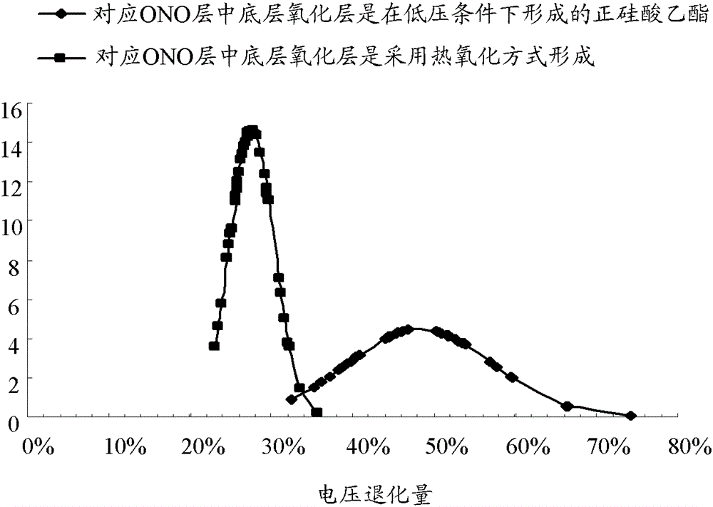
[0040] As mentioned in the background technology section, the accelerated test was used to evaluate the existing 0.5μm OTP device in the laboratory, and the results showed that the degradation of the threshold voltage of the device was far below the expected requirement, and thus the data retention of the device was poor . OTP devices have poor data retention, which means that the charge stored in them is easily lost. After the OTP device is programmed, the programmed data (that is, the charge) is stored in the storage unit of the device. Therefore, in order to make the charge in the storage unit not easy to lose, it is necessary to have a good connection between it and the surrounding components. isolation effect.

[0041] Based on this, the present invention provides a kind of OTP device, and this OTP device comprises: substrate; The storage unit that is positioned on described substrate, described storage unit comprises: gate dielectric layer, floating gate, laminated diel...

Embodiment 2

[0043] The OTP device provided by the present invention will be described in detail below with specific embodiments in conjunction with the accompanying drawings.

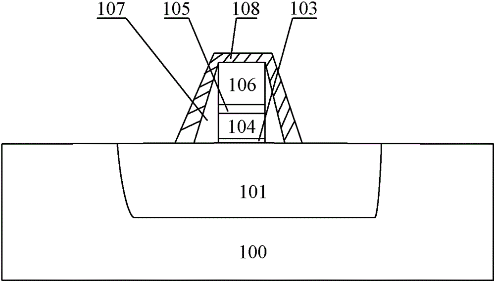
[0044] refer to figure 1 , figure 1 A schematic structural diagram of an OTP device provided by an embodiment of the present invention, the OTP device includes: a substrate 100; a well region 101 located in the substrate 100; a gate dielectric layer 103 located on the well region 101; the gate dielectric layer 103 A floating gate 104, a stacked dielectric layer 105 and a control gate 106 are sequentially arranged on the upper surface, and the well region 101, the gate dielectric layer 103, the floating gate 104, the stacked dielectric layer 105 and the control gate 106 together constitute the memory of the OTP device. unit; the two sides of the storage unit are provided with sidewalls 107, the existence of the sidewalls 107 can prevent the charge in the storage unit from leaking out on the one hand, and on the o...

Embodiment 3

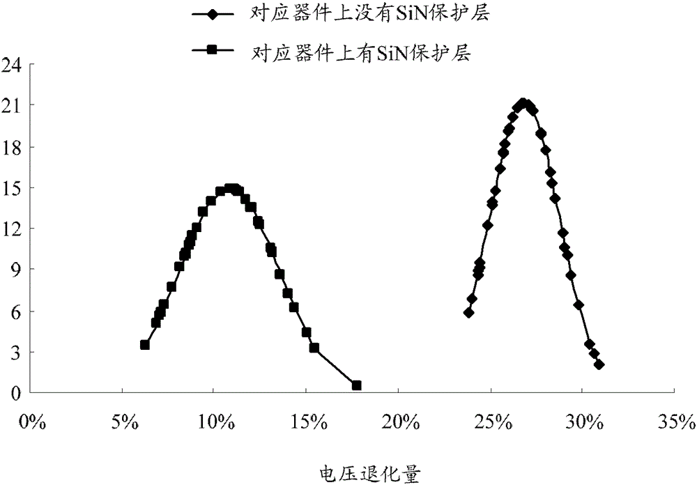
[0055] refer to Figure 5 , the OTP device provided in this embodiment adds a protection gate 109 on the basis of the second embodiment, and the protection gate 109 is located above the control gate 106 and belongs to a part of the memory cell. Since the control gate 106 includes metal silicide (generally tungsten silicide) in addition to the polysilicon gate, the metal silicide is often peeled off in other processes (such as high-temperature processes such as annealing), which will cause the control gate The resistance of 106 becomes higher, the actual working voltage decreases, and affects the performance of the device. Therefore, by forming a protective gate 109 on the control gate 106, the peeling of the metal silicide on the control gate 106 can be prevented, the gate control capability is improved, and the device performance is improved. Data retention of OTP devices.

[0056] The OTP device provided by the present invention has been described in detail above, and the m...


PUM


Abstract

The embodiment of the invention discloses an OTP (one time programmable) device and a manufacturing method thereof. The OTP device comprises a substrate, a storage unit, side walls and protective layers, wherein the storage unit is positioned on the substrate; the storage unit comprises a gate medium layer, a floating gate, a superposed medium layer and a control grate, which are sequentially arrayed from bottom to top; the side walls are arranged at the two sides of the storage unit; and the protective layers are positioned on the storage unit and cover the side walls. According to the OTP (one time programmable) device provided by the invention, the protective layers cover the storage unit and the side walls, the protective layers can stop mobile ions at the periphery of the storage unit from affecting electric charge in the storage unit, and the electric charge in the storage unit is also avoided from leaking, so that the capability of the storage unit on storing electric charge is improved through the protective layers, namely the data retention capability of the OTP device is improved.

Description

technical field [0001] The invention relates to the technical field of semiconductor device manufacturing, and more specifically, relates to an OTP device and a manufacturing method thereof. Background technique [0002] OTP (One Time Programmable, one-time programmable) device is a storage device. Compared with multiple programming, its programming process is an irreversible activity. It is suitable for applications where the program is fixed because the cost is low. And be widely used. [0003] One of the key parameters to measure the reliability of the OTP device is the data retention (data retention) of the OTP device. After the OTP device is programmed, the programmed data (specifically charge) is stored in the storage unit of the OTP device (specifically the floating gate of the storage unit), and the ability of the storage unit to store charge is the value of the OTP device. data retention. If the charge tends to leak from the memory cell, it indicates that the OTP...

Claims


Application Information

Patent Timeline
Patent Type & Authority Patents(China)
IPC IPC(8): H01L27/115H01L21/8247
Inventor 张花威马春霞王德进
Owner CSMC TECH FAB2 CO LTD
Why Eureka
Try Eureka