
Manufacturing method for micro electro mechanical system (MEMS) micromirror bistable state structure and optical switch

A manufacturing method and a bistable technology, applied in the field of optical switches with a bistable structure, can solve problems such as low reliability, affecting device response speed, complicated operation, etc., and achieve the effect of high processing efficiency and easy operation

Active Publication Date: 2013-02-13
无锡微文半导体科技有限公司
View PDF6 Cites 11 Cited by
  • Summary
  • Abstract
  • Description
  • Claims
  • Application Information

AI Technical Summary

Problems solved by technology

Although the above structure can also achieve a bistable effect, in the switching process, the auxiliary effect of an external force is still required to complete the state switching. The operation is relatively complicated and the reliability is low, which will also affect the response speed of the device.
Simultaneously, the making of this bistable mechanism needs two masks, and it is only a bistable mechanism after making, and there is no mirror surface and base required for making the optical path switch at the same time, so that it needs to be used in the process of use. Processes such as reprocessing or reassembly bring inconvenience to use

Method used


Image

  • Manufacturing method for micro electro mechanical system (MEMS) micromirror bistable state structure and optical switch
  • Manufacturing method for micro electro mechanical system (MEMS) micromirror bistable state structure and optical switch
  • Manufacturing method for micro electro mechanical system (MEMS) micromirror bistable state structure and optical switch

Examples


Embodiment Construction

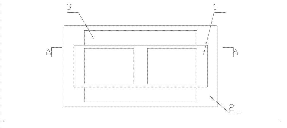
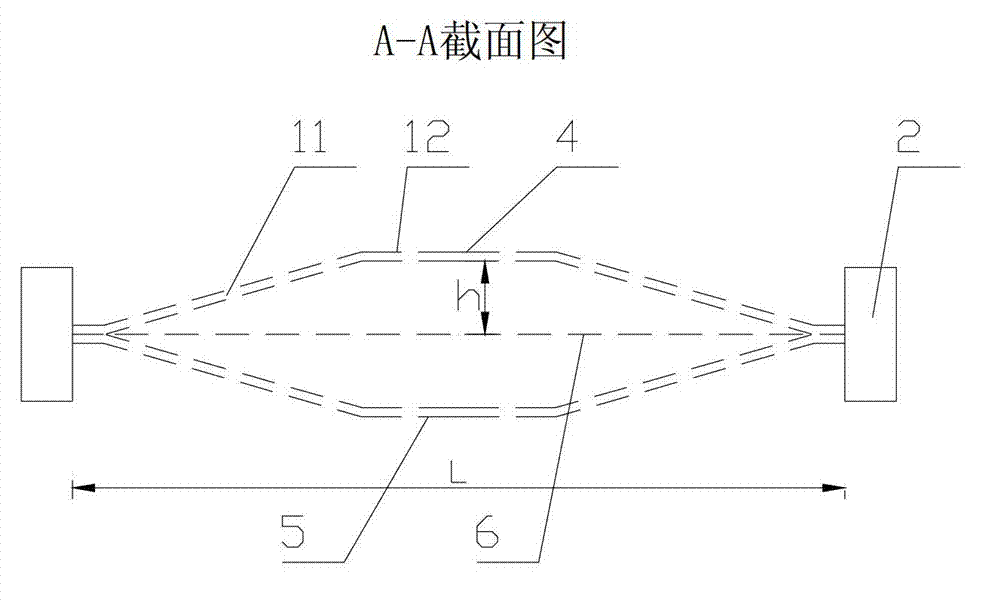
[0033] The technical solutions of the present invention will be further described below in conjunction with the accompanying drawings and through specific implementation methods.

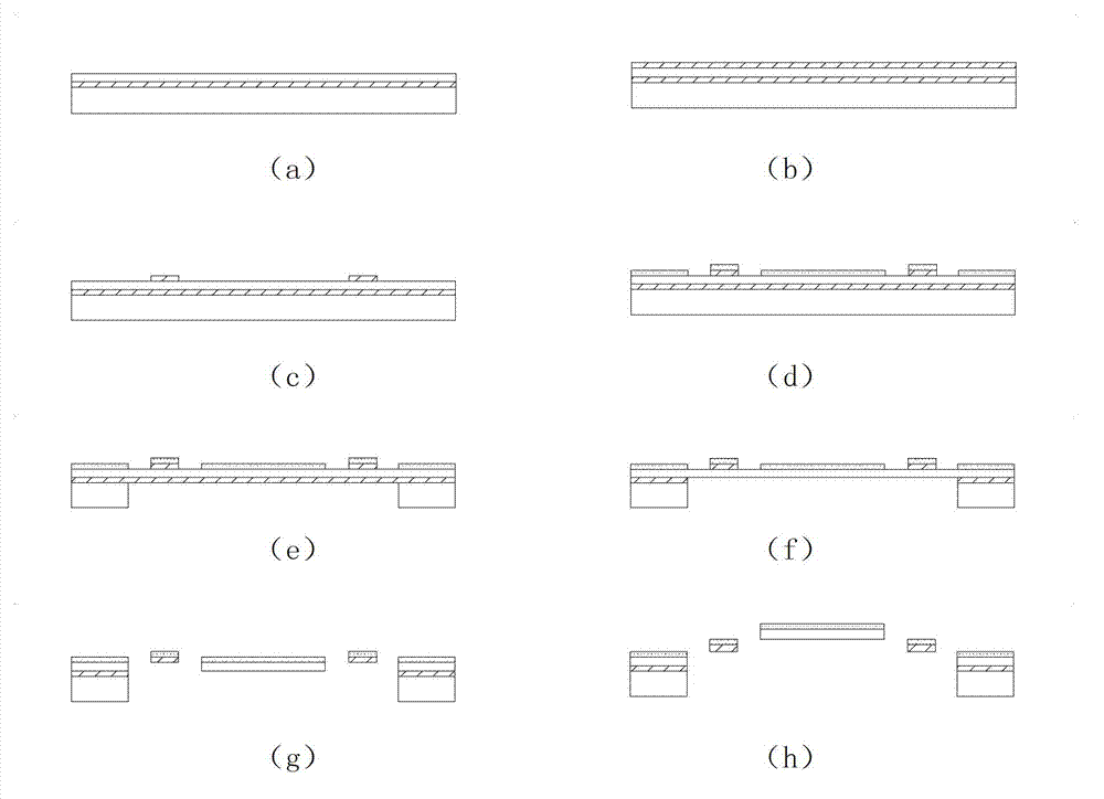
[0034] Such as Figure 1~3 Shown, a kind of manufacture method of MEMS micromirror bistable structure, comprises the following steps:

[0035] Step A: Depositing a first layer of dielectric film material on the front side of the cleaned high-resistance silicon wafer, and etching to form the first material structure layer in the driving arm 11;

[0036] Step B: Evaporate the first layer of metal thin film material on the first material structure layer, and etch to form a metal layer, the metal layer is a layer of material structure in the pad and the driving arm 11, and the metal layer is the same as that formed in step A The first layer of material structure layer forms the driving arm 11;

[0037] Step C: sputtering a second layer of metal thin film on the metal layer formed in step B, and formin...


PUM


Abstract

The invention discloses a manufacturing method for a micro electro mechanical system (MEMS) micromirror bistable state structure. The method comprises the following steps of: depositing a first-layer dielectric thin film material on the front of a high-impedance silicon slice and etching; evaporating a first-layer metal thin material and etching to form a metal layer; sputtering a second-layer metal film and etching to form a micromirror surface; performing deep silicon etching on the back of the silicon slice to form a cavity; performing deep silicon etching on the front of the high-impedance silicon slice; and after etching, cooling to room temperature to form the initial state of the bistable state structure. An optical switch which has the MEMS micromirror bistable state structure which is manufactured by the method comprises the bistable state structure and a drive structure; and the bistable state structure is arranged above the drive structure. The manufacturing process is simple and practicable; the micromirror surface, a straight beam drive arm, and a foundation are integrally formed; and high manufacturing accuracy can be guaranteed; and the optical switch is convenient to operate, high in response speed and reliability and low in energy consumption, and two states are switched by solenoid drive.

Description

technical field [0001] The invention belongs to the field of micro-electromechanical systems, and relates to a manufacturing method of a MEMS micromirror bistable structure and an optical switch including the bistable structure prepared by the method. Background technique [0002] MEMS (Micro-electro-mechanical systems), that is, micro-electro-mechanical systems, are various micro-devices or systems manufactured by micro-processing technology, mainly including micro-structures, micro-sensors, micro-actuators and corresponding processing circuits. It is a high-tech cutting-edge discipline developed on the basis of integrating various micro-processing technologies and applying the latest achievements of modern information technology. Compared with traditional machinery, MEMS devices are smaller in size, the largest is no more than 1cm, or even only a few μm; therefore, it adopts a generation technology similar to integrated circuits (ICs), and utilizes mature technologies and ...

Claims


Application Information

Patent Timeline
IPC IPC(8): G02B26/08B81C1/00B81B7/02
Inventor 陈巧谢会开
Owner 无锡微文半导体科技有限公司
Learn More