Test device and manufacturing method thereof, semiconductor device and manufacturing method thereof

A technology for testing devices and manufacturing methods, applied in semiconductor/solid-state device manufacturing, semiconductor devices, semiconductor/solid-state device components, etc., can solve problems such as chip scrapping, achieve the effect of improving yield and ensuring performance stability

Active Publication Date: 2016-06-29
SHANGHAI HUAHONG GRACE SEMICON MFG CORP
View PDF6 Cites 0 Cited by
  • Summary
  • Abstract
  • Description
  • Claims
  • Application Information

AI Technical Summary

Problems solved by technology

[0009] However, after dicing along the dicing line including the above-mentioned test devices, the electrical properties of the corresponding chips changed greatly, resulting in the scrapping of the chips in the entire wafer

Method used


Image

  • Test device and manufacturing method thereof, semiconductor device and manufacturing method thereof
  • Test device and manufacturing method thereof, semiconductor device and manufacturing method thereof
  • Test device and manufacturing method thereof, semiconductor device and manufacturing method thereof

Examples


Embodiment Construction

[0044] In order to make the above objects, features and advantages of the present invention more comprehensible, specific implementations of the present invention will be described in detail below in conjunction with the accompanying drawings.

[0045] In the following description, many specific details are set forth in order to fully understand the present invention, but the present invention can also be implemented in other ways than those described here, so the present invention is not limited by the specific embodiments disclosed below.

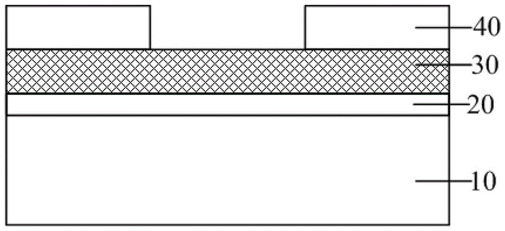
[0046] As mentioned in the background technology section, the channel region of the prior art wafer includes one or more test devices. When the chip is divided along the channel region, the electrical performance of the chip changes greatly compared with that before division. , resulting in the chip being unusable and eventually making the entire wafer scrapped.

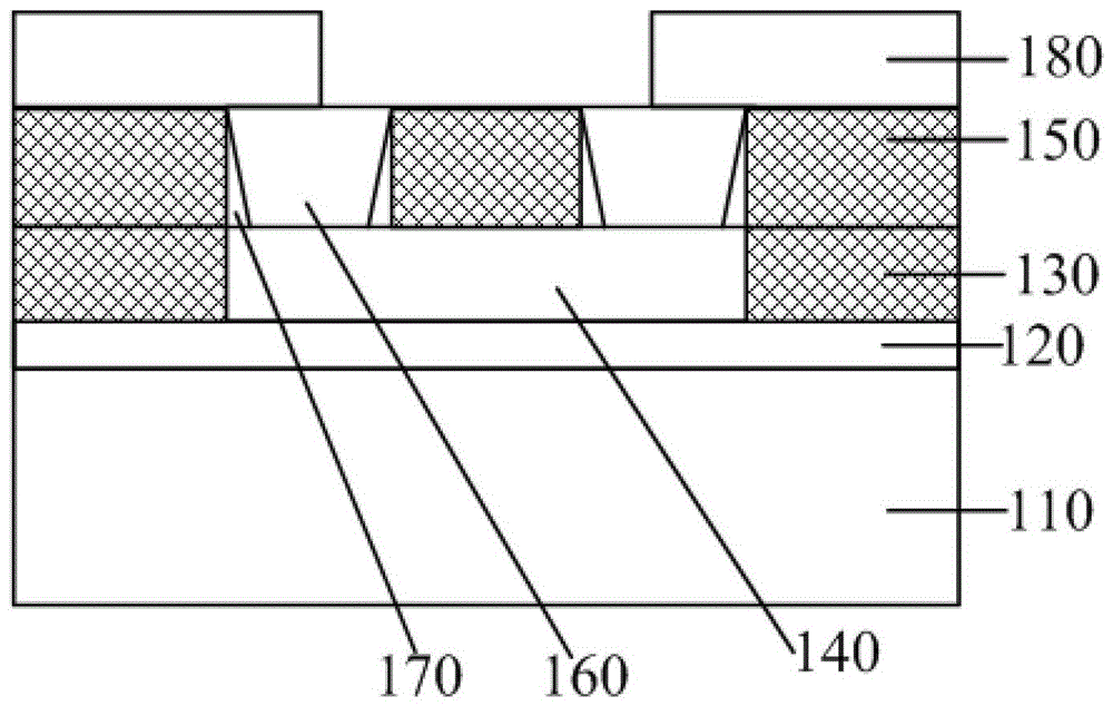
[0047]After research, the inventor found that the reason for this is that t...


PUM


Abstract

The invention discloses a test device, a test device manufacturing method, a semiconductor device and a semiconductor device manufacturing method. The test device comprises a semiconductor substrate, a dielectric layer positioned on the semiconductor substrate and an electrical connecting line positioned on the dielectric layer, wherein the dielectric layer is made from silicon oxide formed by adopting TEOS (tetraethyl orthosilicate) as a reaction source; the dielectric layer comprises metal plugs and dummy contacts; the dummy contacts can be made of tungsten; the ratio of the upper surface area of the dummy contacts to the upper surface area of the whole dielectric layer is greater than or equal to 20 percent; and the electrical connecting line can be made of copper, aluminum or copper aluminum alloy. The semiconductor device comprises a plurality of dies and cutting channels positioned between the dies, and the cutting channels comprise the test devices. According to the invention, the adhesive force between the electrical connecting line and the dielectric layer of the test device can be increased and finally the stable performance of the semiconductor device can be ensured.

Description

technical field [0001] The invention relates to the technical field of semiconductors, in particular to a testing device and a manufacturing method thereof, a semiconductor device and a manufacturing method thereof. Background technique [0002] In the field of semiconductor manufacturing, multiple chips (Die) with the same structure are usually manufactured simultaneously on a semiconductor wafer, and the area between adjacent chips is a dicing line. In order to ensure the reliability of semiconductor devices, multiple test devices are usually fabricated in the dicing line for testing some key parameters (such as: RS resistance value). Different semiconductor devices may need to obtain different test parameters, and different test parameters may require different test devices. When the chip manufacturing process is completed and the test devices in the dicing lanes meet the requirements, the wafer can be cut along the predetermined dicing lanes to form discrete chips, and ...

Claims


Application Information

Patent Timeline
Patent Type & Authority Patents(China)
IPC IPC(8): H01L23/544H01L21/02
Inventor 李秀莹刘宇王鹏
Owner SHANGHAI HUAHONG GRACE SEMICON MFG CORP
Why Eureka
Try Eureka