Vacuum sealing packaging structure and packaging method for infrared focal plane detector chip

A technology for vacuum sealing packaging and detector chips, which is applied in radiation control devices and other directions, can solve the problems that the packaging structure is difficult to meet application requirements, and achieve the effects of effective thermal insulation structure, reducing packaging cost, and reducing volume

Active Publication Date: 2013-03-06
YANTAI RAYTRON TECH
View PDF3 Cites 19 Cited by
  • Summary
  • Abstract
  • Description
  • Claims
  • Application Information

AI Technical Summary

Problems solved by technology

Moreover, for some infrared focal plane detector chips, in some cases, they need to work in an environment with good thermal insulat

Method used


Image

  • Vacuum sealing packaging structure and packaging method for infrared focal plane detector chip
  • Vacuum sealing packaging structure and packaging method for infrared focal plane detector chip
  • Vacuum sealing packaging structure and packaging method for infrared focal plane detector chip

Examples


Embodiment Construction

[0030] The principles and features of the present invention are described below in conjunction with the accompanying drawings, and the examples given are only used to explain the present invention, and are not intended to limit the scope of the present invention.

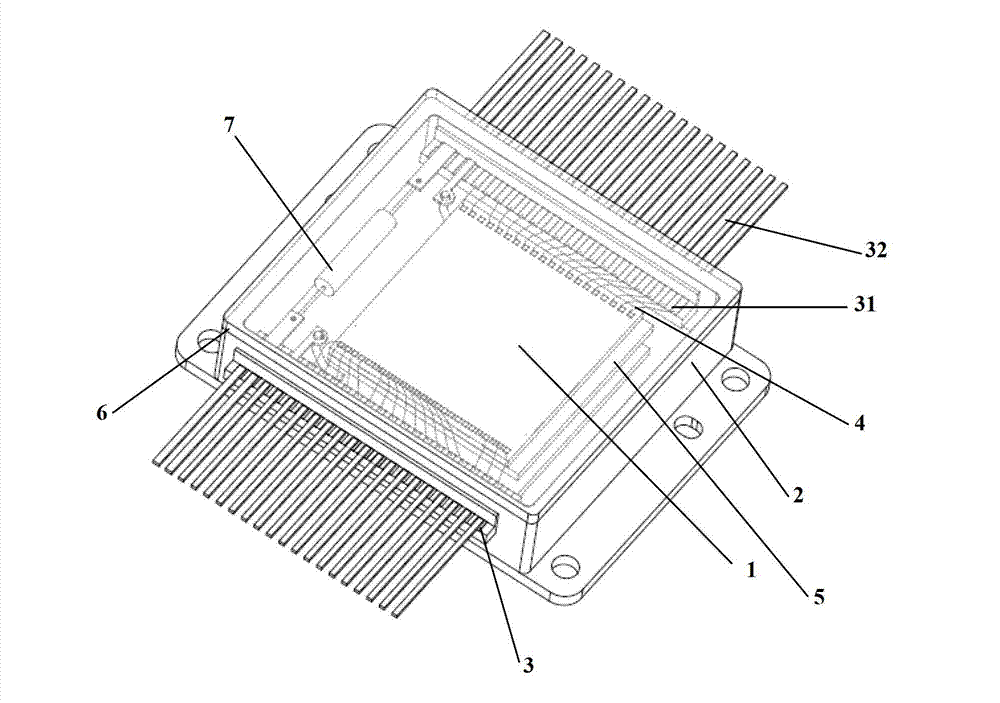
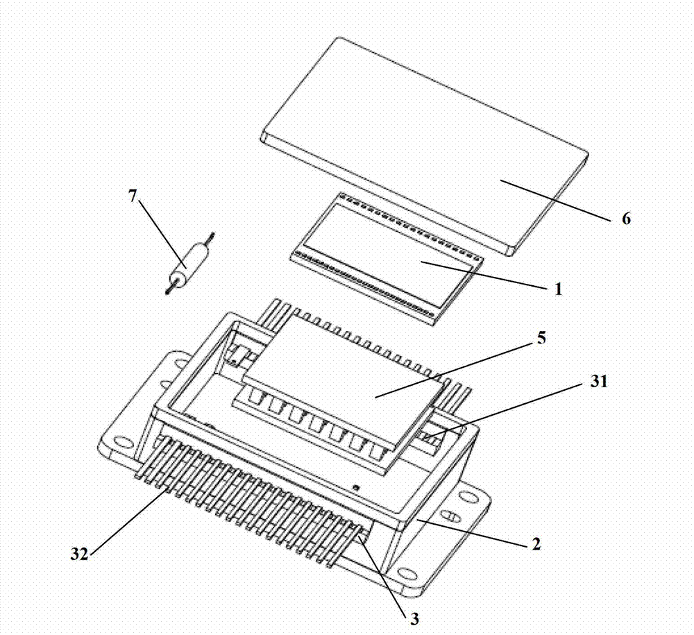
[0031] Such as figure 1 and figure 2 As shown, the existing high-vacuum packaging technology for infrared focal plane array detectors uses a metal shell as a sealed cavity. The shell 2 is an open cuboid cavity, and ceramic structural parts 3 are made on its side walls. Ceramic structural parts 3 The metal pad 31 is made on the ceramic structural part 3, and the metal pad 31 is connected with the metal lead attached to the ceramic structural part 3 outside the side wall of the housing 2. 32 is electrically connected. In this way, the infrared focal plane detector chip 1 is electrically connected to the outside through the gold wire 4 to realize signal communication and control. The infrared focal plane detector chi...


PUM


Abstract

The invention relates to a vacuum sealing packaging structure and a packaging method for an infrared focal plane detector chip. The packaging method comprises the following specific steps of: firstly, mounting the infrared focal plane detector chip and a getter in a chamber of a packaging casing and enabling the getter to be positioned between the infrared focal plane detector chip and the bottom of the packaging casing; and secondly, connecting an optical window with the packaging casing in a sealing manner to form a vacuum sealing chamber. According to the vacuum sealing packaging structure and the packaging method disclosed by the invention, the volume of the vacuum sealing packaging structure of the infrared focal plane detector chip is remarkably reduced; a traditional parallel mounting mode of the infrared focal plane detector chip and the getter is changed into a vertical mounting mode; and the requirement of portable infrared thermal imaging application to the packaging structure of the infrared focal plane detector chip on miniaturization is met. In addition, the packaging structure also provides a concise and effective thermal insulating structure and realizes an insulated work mode of the concise and effective thermal insulating structure; and the packaging structure is concise in structure and low in cost.

Description

technical field [0001] The invention relates to the field of semiconductor optoelectronics, in particular to a vacuum-sealed packaging structure and packaging method for an infrared focal plane detector chip. Background technique [0002] Infrared imaging technology is more and more widely used in industrial sensing, image monitoring, automobile industry, fire search and rescue, and even military navigation and night vision. Infrared focal plane detector manufacturing technology is the core of thermal imaging technology, and infrared focal plane array detector chip sealing packaging technology is the key link to realize infrared detector imaging. Infrared focal plane array detector chip needs to be in a sealed environment under vacuum Otherwise, the imaging function of its bolometer cannot be exerted. Generally speaking, the high-vacuum packaging technology of infrared focal plane array detectors uses a metal shell as a sealed cavity, and its typical structure is as follows...

Claims


Application Information

Patent Timeline
IPC IPC(8): H01L27/146
Inventor 熊笔锋马宏王宏臣江斌
Owner YANTAI RAYTRON TECH
Why Eureka
Try Eureka