Limit mold for back lapping of infrared focal plane detector and preparation method

An infrared focal plane and detector technology, applied in the direction of manufacturing tools, semiconductor devices, stone processing equipment, etc., can solve the problem that the reserved thickness of the chip cannot be accurately controlled within the deviation range, and the consistency and uniformity of the chip thickness of the module cannot be guaranteed. Complex layer operations and other issues, to avoid uncontrollable operations, ensure consistency and uniformity, and wide applicability

Active Publication Date: 2013-03-13
SHANGHAI INST OF TECHNICAL PHYSICS - CHINESE ACAD OF SCI
View PDF3 Cites 5 Cited by
  • Summary
  • Abstract
  • Description
  • Claims
  • Application Information

AI Technical Summary

Problems solved by technology

[0004] There are many shortcomings in the above method: first, the consistency and uniformity of the chip thickness of each focal plane module cannot be guaranteed; Accumulate multiple layers of accompanying sheets. After each layer of accompanying sheets is pasted and fixed, it is easy to cause the interlayer movement of the accompanying sheets when the wax is melted again, making the operation complicated and uncontrollable; finally, the preparatory work of the early stage and the cleaning of the middle and lower layers of the accompanying sheets Large volume, low work efficiency

Method used


Image

  • Limit mold for back lapping of infrared focal plane detector and preparation method
  • Limit mold for back lapping of infrared focal plane detector and preparation method
  • Limit mold for back lapping of infrared focal plane detector and preparation method

Examples


Embodiment Construction

[0028] The implementation of this patent will be described in detail below by taking a mercury cadmium telluride infrared focal plane device with a photosensitive element array of 32x4 as an example:

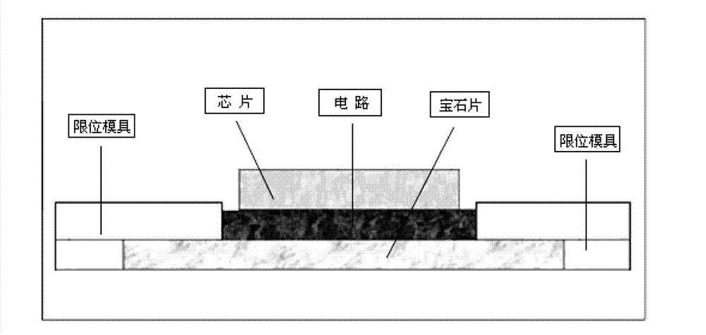
[0029] The upper chip of the 32x4 HgCdTe infrared focal plane device in this example is made of GaAs substrate material, the readout circuit of the middle layer is made of Si-based material, and the substrate material is gemstone. The thickness of the GaAs substrate is 350 μm, the thickness of the intermediate circuit is 450 μm, and the thickness of the lower gemstone substrate is 330 μm. According to the project requirements, the thickness of the final chip reserved is 20 μm.

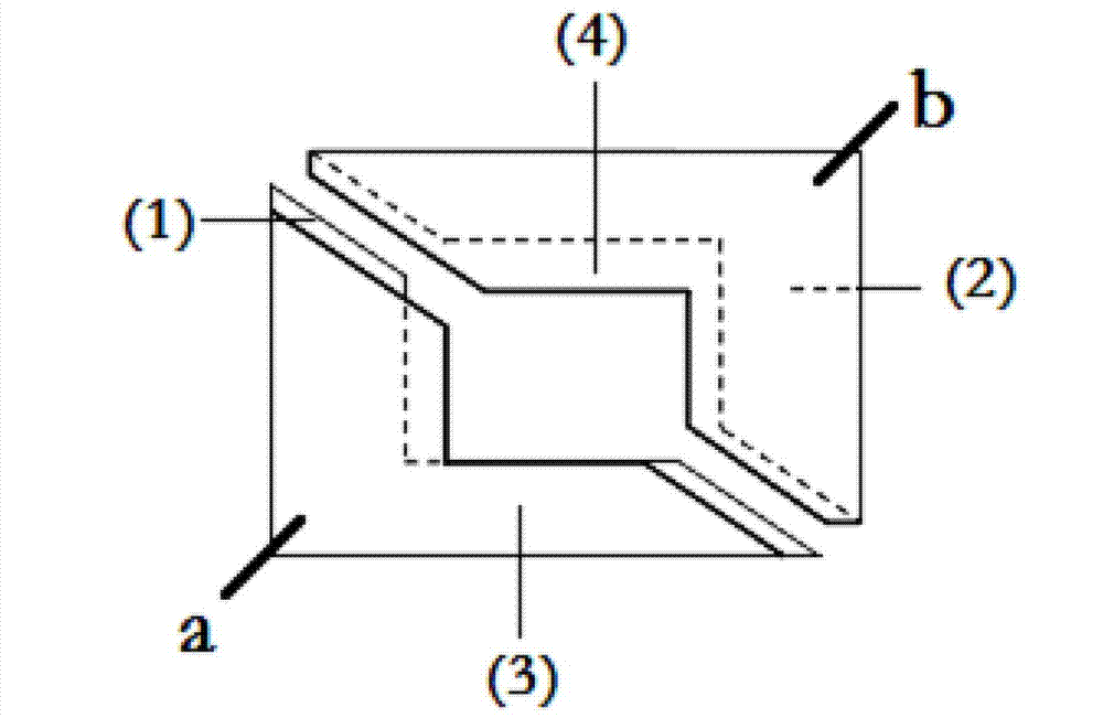
[0030] The method for controlling the thinning thickness of the back of the infrared focal plane detector according to the present invention is used to prepare corresponding limiting molds according to the specific specifications of the 32x4 focal plane module.

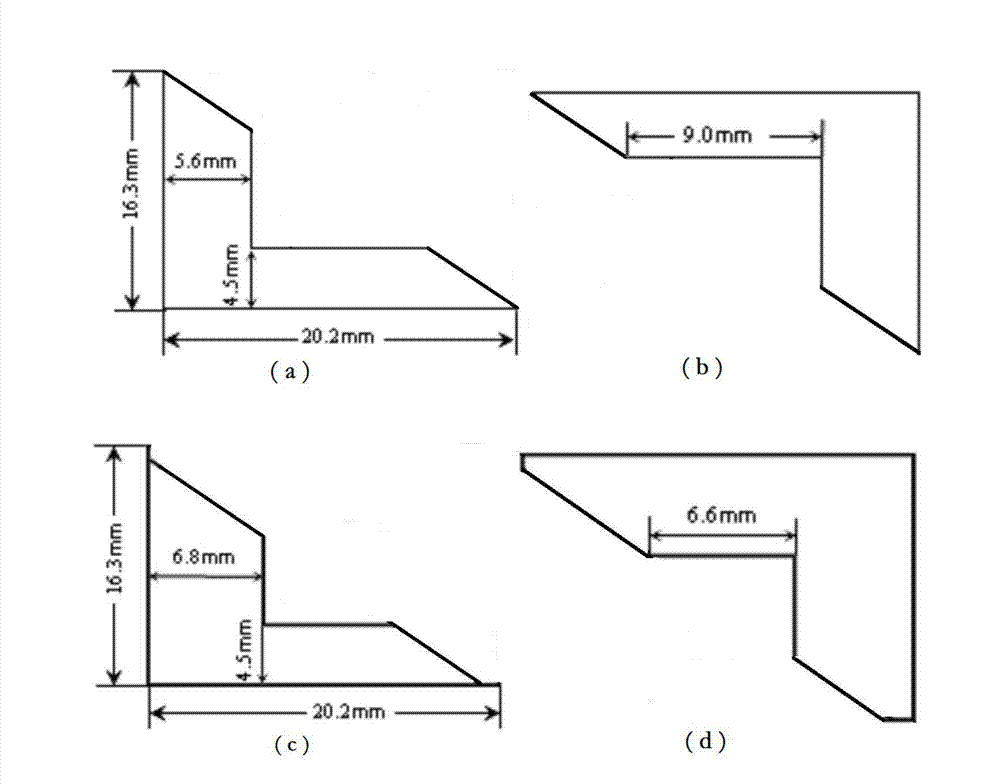
[0031] First, choose two rectangular whi...


PUM


Abstract

The invention discloses a limit mold for back lapping of an infrared focal plane detector and a preparation method. Uniformity and homogeneity of thicknesses of detector chips can be accurately controlled due to the special limit design of the limit mold, the limit mold is mainly made of two diamond pieces with very large hardness, the back lapping and polishing condition of the detector chips almost has no effect on the diamond pieces, rectangular holes are opened at the centers of the two diamond pieces through a laser according to the feature size of the detector and the mold is divided into two portions along the diagonals of the rectangular holes through Disco cutting, and special DW3 low-temperature gum is used for bonding and curing the two layers. According to the limit mold, raw materials are simple and easy to obtain, accurate thickness control is provided, the technological process is controllable, the operation processes are few, and the mold can be recycled and has wide applicability.

Description

technical field [0001] The invention relates to the field of infrared focal plane detector manufacturing, in particular to a device preparation process for an infrared focal plane detector, specifically a limiting mold and a preparation method used in the device back thinning process. Background technique [0002] The infrared focal plane detector is composed of a chip (infrared photosensitive element), a readout circuit and a gemstone substrate flip-welded interconnection. The back thinning of the focal plane detector is to obtain the chip thickness and optical surface that match the optical system within the deviation range, reduce the internal stress on the photosensitive element of the chip, improve the low-temperature reliability of the device, and also improve the back-illuminated type. Backside transmission of HgCdTe infrared focal plane detectors. Therefore, the back thinning process of the focal plane detector is a key basic process technology that affects device p...

Claims


Application Information

Patent Timeline
Patent Type & Authority Applications(China)
IPC IPC(8): H01L31/18B28D5/00
Inventor 钟艳红廖清君曹菊英王建新吴廷琪俞君吴云杨勇斌何高胤
Owner SHANGHAI INST OF TECHNICAL PHYSICS - CHINESE ACAD OF SCI
Why Eureka
Try Eureka