MOS device provided with vertical GaAs base structure and fabrication method of MOS device

A MOS device and vertical structure technology, applied in semiconductor/solid-state device manufacturing, semiconductor devices, electrical components, etc., can solve problems such as difficult to obtain breakthroughs, achieve the effects of simplifying the manufacturing process, increasing switching speed, and realizing selective corrosion

Inactive Publication Date: 2013-03-20
INST OF MICROELECTRONICS CHINESE ACAD OF SCI
View PDF4 Cites 5 Cited by
  • Summary
  • Abstract
  • Description
  • Claims
  • Application Information

AI Technical Summary

Problems solved by technology

At present, due to the limitation of the silicon material itself, the characteristics of Trench MOS devices, especially the compromise between the maximum operating voltage and the conduction current, have been difficult to obtain a breakthrough

Method used


Image

  • MOS device provided with vertical GaAs base structure and fabrication method of MOS device
  • MOS device provided with vertical GaAs base structure and fabrication method of MOS device
  • MOS device provided with vertical GaAs base structure and fabrication method of MOS device

Examples


Embodiment Construction

[0025] In order to make the object, technical solution and advantages of the present invention clearer, the present invention will be described in further detail below in conjunction with specific embodiments and with reference to the accompanying drawings.

[0026] The GaAs-based vertical structure MOS device and its manufacturing method provided by the present invention reduce the on-resistance of the device by utilizing the high electron mobility characteristics of III-V semiconductor materials; through the design of the InGaP layer, the gate groove is realized. Selective etching in etching, thereby improving the consistency and process stability in the device manufacturing process.

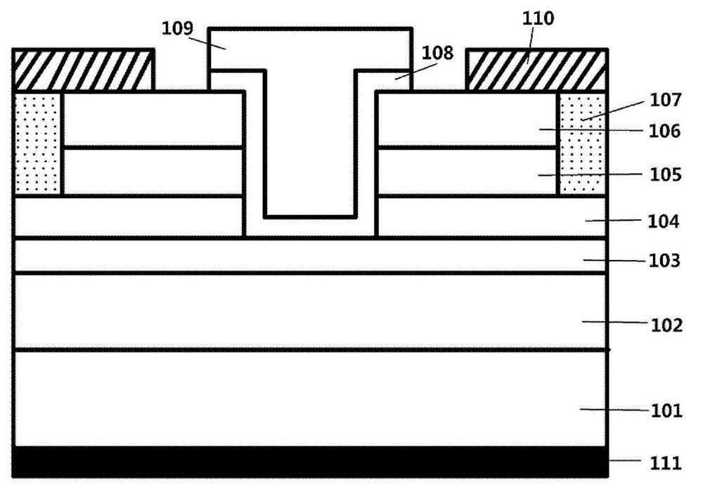
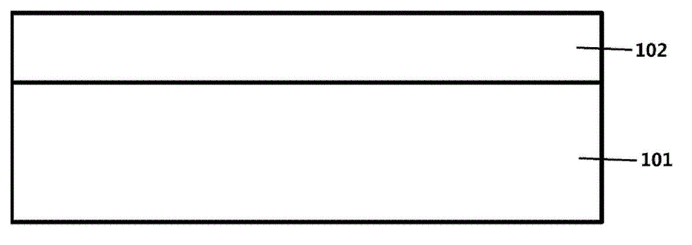
[0027] Such as figure 1 as shown, figure 1 A schematic diagram showing a GaAs-based vertical structure MOS device according to an embodiment of the present invention, the GaAs-based vertical structure MOS device includes: an N-type GaAs substrate layer 101; an N-type low-doped N-type substrat...


PUM


Abstract

The invention discloses an MOS (metal oxide semiconductor) device provided with a vertical GaAs base structure, and a fabrication method of the MOS device. The MOS device provided with the vertical GaAs base structure comprises an N-type GaAs substrate layer, an N-type GaAs lightly doped layer formed on the N-type GaAs substrate layer, an N-type InGaP lightly doped layer formed on the N-type low GaAs doped layer, an N-type GaAs doped layer formed on the N-type InGaP lightly doped layer, a P-type group III-V semiconductor channel layer formed on the N-type GaAs doped layer, a highly doped group III-V semiconductor ohmic contact layer formed on the P-type group III-V semiconductor channel layer, P-type areas formed in the P-type group III-V semiconductor channel layer and the ohmic contact layer, a gate groove structure formed above the N-type InGaP lightly doped layer and in the N-type GaAs lightly doped layer, the P-type group III-V semiconductor channel layer and the ohmic contact layer, a gate dielectric layer formed in the gate groove structure, a gate metal electrode formed on the gate dielectric layer, source metal electrodes formed on the ohmic contact layer and the P-type areas, and a drain metal electrode formed on the back of the N-type GaAs substrate layer.

Description

technical field [0001] The invention relates to the technical field of semiconductor integrated circuit manufacturing, in particular to a GaAs-based vertical structure MOS device and a manufacturing method thereof. Background technique [0002] Compared with silicon materials, III-V compound semiconductor materials have the advantages of high carrier mobility, large forbidden band width, etc., and have good characteristics in thermal, optical and electromagnetic aspects. In recent years, due to the rapid progress in the research of atomic layer deposition technology and III-V MOSFET devices, MOSFETs using IIIV semiconductor materials as channel materials and ALD dielectrics as gate dielectrics have achieved good electrical characteristics, which is a great opportunity for manufacturing Surface devices of III-V semiconductors with different structures laid the technical foundation. Trench MOS device is a power device, which has higher on-state current, lower on-resistance, a...

Claims


Application Information

Patent Timeline
Patent Type & Authority Applications(China)
IPC IPC(8): H01L29/78H01L29/06H01L29/20H01L21/336
Inventor 刘洪刚常虎东刘桂明
Owner INST OF MICROELECTRONICS CHINESE ACAD OF SCI
Why Eureka
Try Eureka