Duty ratio adjusting circuit

A technology for adjusting circuit and duty cycle, applied in electrical components, generating electrical pulses, pulse generation, etc., can solve the problems that the clock signal cannot reach the duty cycle, the adjustment circuit is complicated, the charging time and the discharging time are not equal, etc. Achieve the effect of low cost and simple structure

Inactive Publication Date: 2013-03-20
SHANGHAI HUAHONG GRACE SEMICON MFG CORP
View PDF4 Cites 19 Cited by
  • Summary
  • Abstract
  • Description
  • Claims
  • Application Information

AI Technical Summary

Problems solved by technology

Therefore, the clock signal output by the RO depends to a large extent on factors such as process conditions, temperature, and the operating voltage of the RO, which will make the duty cycle of the final clock signal output by the RO less than 50%, resulting in the charge pump CPB The charging time and discharging time of capacitor C6 are not equal,

Method used


Image

  • Duty ratio adjusting circuit
  • Duty ratio adjusting circuit
  • Duty ratio adjusting circuit

Examples


Embodiment 1

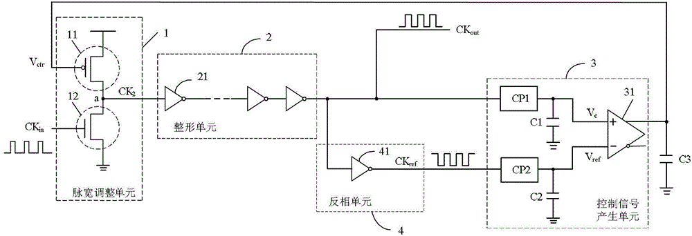
[0044] image 3 It is a circuit diagram of the duty cycle adjustment circuit of the first embodiment of the present invention.

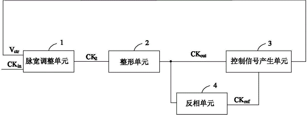
[0045] Such as image 3 As shown, the duty cycle adjustment circuit includes: a pulse width adjustment unit 1, a shaping unit 2, a control signal generation unit 3, and an inversion unit 4.

[0046] Wherein, the pulse width adjustment unit 1 includes: a first transistor 11 and a second transistor 12;

[0047] The gate of the first transistor 11 inputs a control signal V ctr , The gate of the second transistor 12 inputs the first clock signal CK in ;

[0048] The drain of the first transistor 11 is connected to the drain of the second transistor 12 to output a second clock signal CK 2 ;

[0049] The source of the first transistor 11 is connected to a first voltage source, and the source of the second transistor 12 is connected to a second voltage source.

[0050] Wherein, the shaping unit 2 includes: an odd number of inverters 21 connected in series, and the s...

Embodiment 2

[0087] In this embodiment, the duty cycle adjustment circuit is similar to that in Embodiment 1. The difference is that the shaping unit in this embodiment includes an even number of inverters, and the connection mode of the amplifier in the control signal generating unit is the same as in Embodiment 1. Different.

[0088] Image 6 It is a circuit diagram of the duty cycle adjustment circuit of the second embodiment of the present invention.

[0089] Such as Image 6 As shown, the duty cycle adjustment circuit includes: a pulse width adjustment unit 1, a shaping unit 2', a control signal generation circuit 3', and an inversion unit 4.

[0090] The pulse width adjusting unit 1 and the inverting unit 4 are the same as or similar to those in the first embodiment, and will not be repeated here. The shaping unit 2'includes an even number of inverters 21, and the structures of the first charge pump CP1 and the second charge pump CP2 included in the control signal generating unit 3'are sim...


PUM


Abstract

The invention provides a duty ratio adjusting circuit which is used for adjusting the duty ratio of a first clock signal to acquire a third clock signal. The duty ratio adjusting circuit comprises a pulse width adjusting unit, a shaping unit, an inverse phase unit and a control signal generating unit, wherein the pulse width adjusting unit inputs a second clock signal and outputs the third clock signal; the inverse phase unit inputs the third clock signal and outputs a fourth clock signal; the third clock signal and the fourth clock signal have opposite phase position; and the control signal generating unit inputs the third clock signal and the fourth clock signal and outputs a control signal. The duty ratio adjusting circuit is simple in structure and can stably output the clock signal with the expected duty ratio.

Description

Technical field [0001] The present invention relates to the technical field of integrated circuits, in particular to a duty cycle adjustment circuit which is not affected by manufacturing process, voltage and temperature parameters. Background technique [0002] With the continuous development of integrated circuit technology, the working speed of the chip continues to increase, and the increase in working speed means more stringent timing accuracy. Therefore, the requirements for system clock performance are also constantly improving. The duty cycle of the clock is a relatively important performance index in the clock performance. Duty Cycle usually refers to the ratio of the duration of a positive pulse to the pulse period in a series of ideal pulse cycle sequences (such as a square wave). For example, a duty cycle of 50% means that the width of the high-level clock cycle is equal to the width of the low-level clock cycle. For now, a 50% duty cycle is more beneficial to data ...

Claims


Application Information

Patent Timeline
IPC IPC(8): H03K3/017
Inventor 陈丹凤
Owner SHANGHAI HUAHONG GRACE SEMICON MFG CORP
Why Eureka
Try Eureka