

Photovoltaic solar cell and method for producing a photovoltaic solar cell
A solar cell and photovoltaic technology, applied in photovoltaic power generation, final product manufacturing, sustainable manufacturing/processing, etc., can solve problems such as expensive processes and high costs, and achieve the effect of simplifying costs and manufacturing methods
- Summary
- Abstract
- Description
- Claims
- Application Information
AI Technical Summary
Problems solved by technology
Method used
Image

Examples
Embodiment Construction
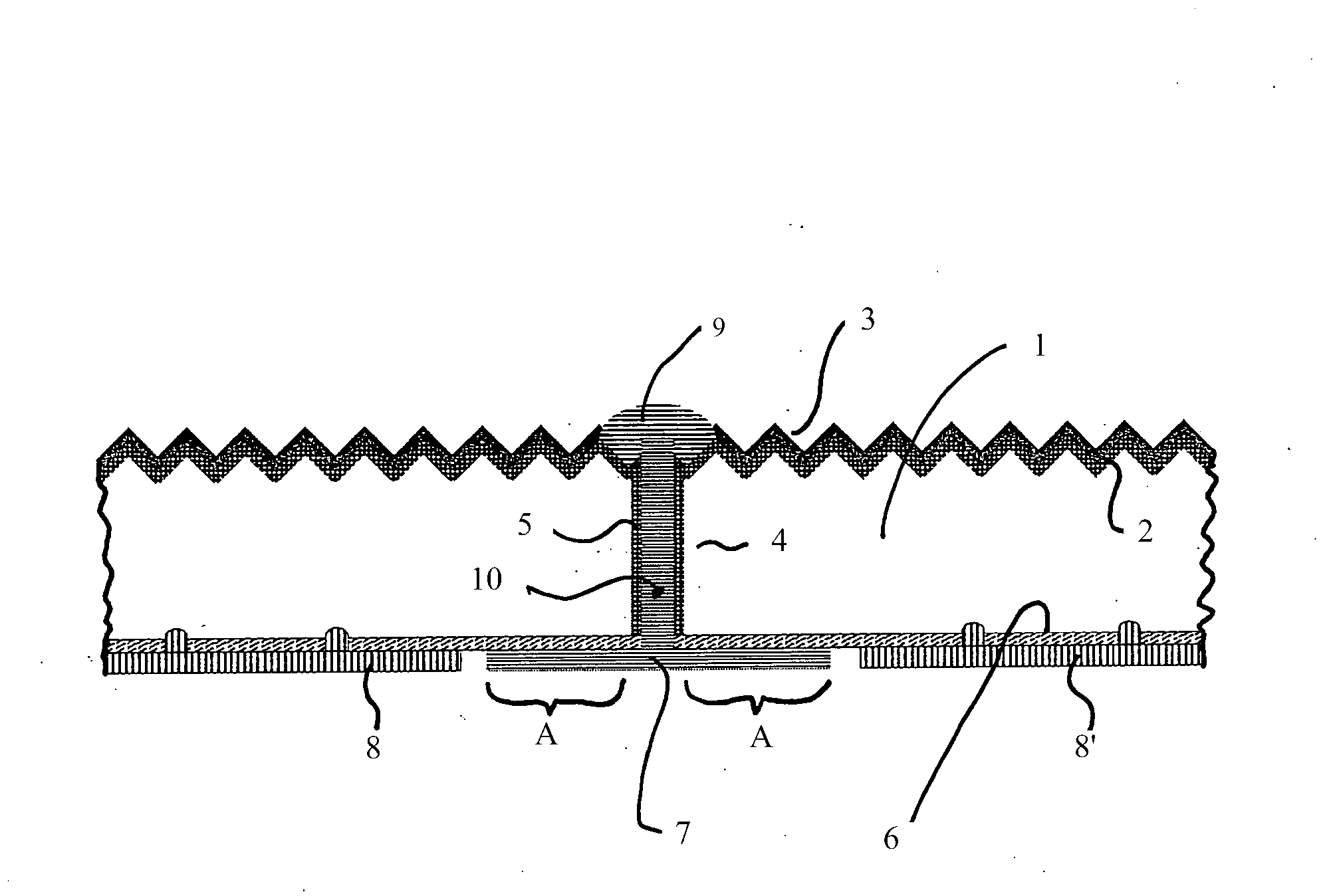
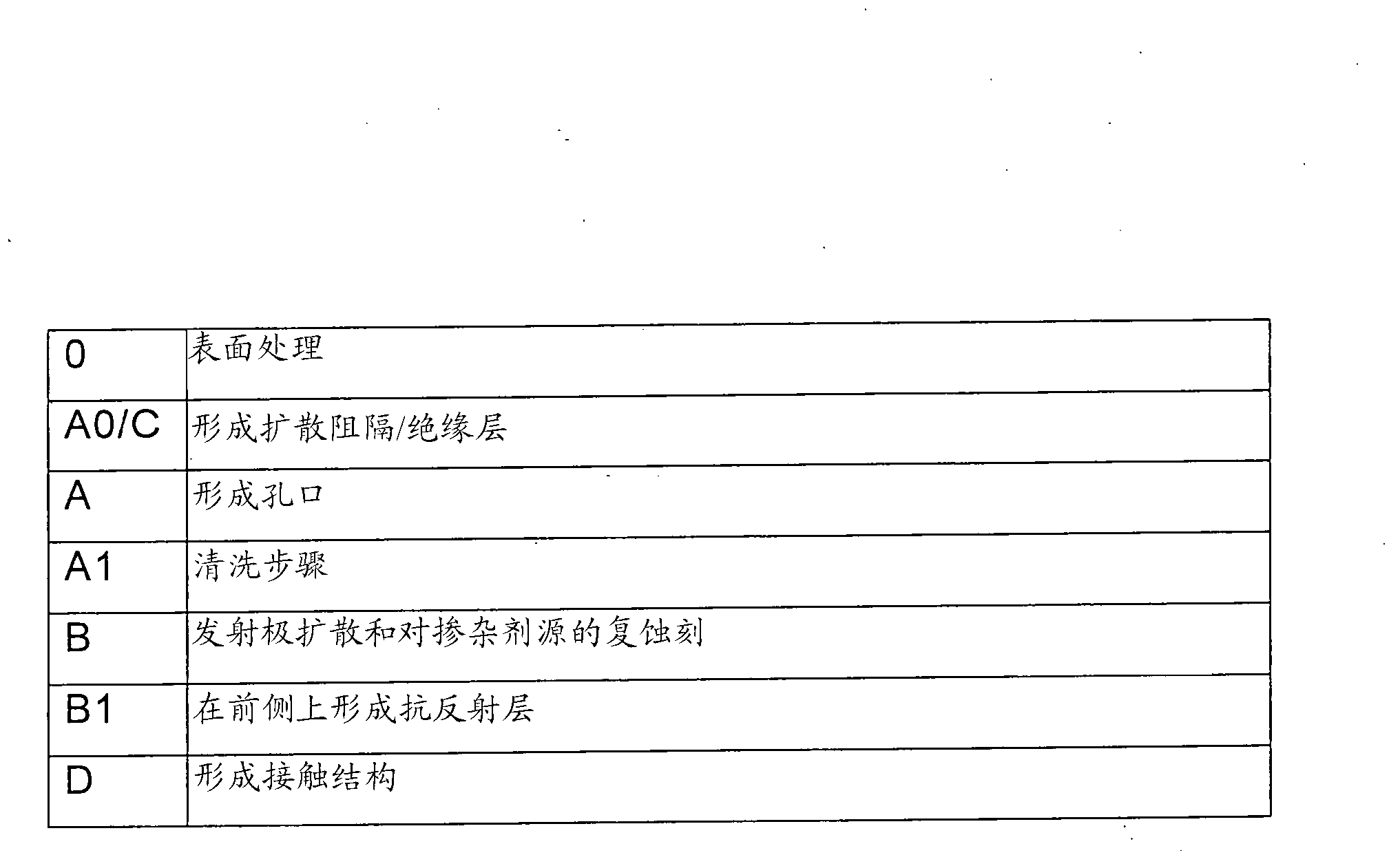
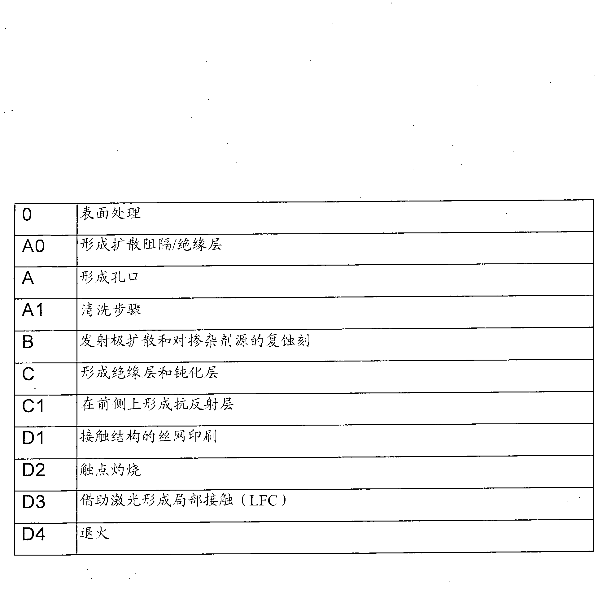
[0072] exist figure 1 The embodiment of the solar cell according to the invention shown in the following by means of image 3 Manufactured by the process described in .
[0073] exist figure 1 The solar cell according to the invention in the present invention comprises a P-doped semiconductor substrate 1 formed as a monocrystalline silicon wafer or a polycrystalline silicon wafer with a base resistance of 0.1 ohm-cm to 10 ohm-cm. exist figure 1 The front side emitter region 2 is formed on the front side shown in the upper middle. The front side has a texture to increase the light coupling, and in order to increase the light coupling, an antireflection layer 3 in the form of a silicon nitride layer with a thickness of approximately 70 nm is additionally arranged on the front side of the semiconductor substrate 1 .
[0074] figure 1 Only a part of a solar cell according to the invention with only one opening 4 is shown. The solar cell extends left and right in a mirror ima...
PUM
 Abstract
Description
Claims
Application Information