Method for preparing substructure less than 10 nanometers on nanometer material surface
A technology of nanomaterials and substructures, applied in the manufacture of microstructure devices, processes for producing decorative surface effects, microstructure technology, etc., can solve the problems of reducing manufacturing efficiency and increasing manufacturing costs, and achieve the effect of convenient operation
- Summary
- Abstract
- Description
- Claims
- Application Information
AI Technical Summary
Problems solved by technology
Method used
Image


Examples
Embodiment 1
[0024] Embodiment 1: a kind of method that prepares substructure below 10 nanometers on the nanomaterial surface, this method comprises the steps:
[0025] 1) Choose zinc oxide nanowires with good crystallization and diameter less than 50 nanometers; the length of zinc oxide nanowires is not limited;
[0026] 2) The above-mentioned nanowires are supported on a copper mesh; the copper mesh used is a commercially available copper mesh for TEM experiments, generally with a diameter of 3 mm and a mesh size of 200-2000 mesh;
[0027] 3) Put the supported nanowires into the sample rod of the electron microscope (TEM), then insert it into the vacuum chamber of the TEM, and evacuate until the electron gun can work normally; the vacuum degree of the vacuum chamber is 5.0±1.0×10 -5 Pa;
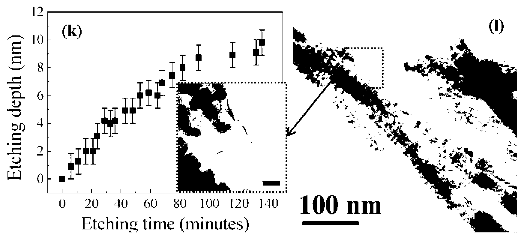
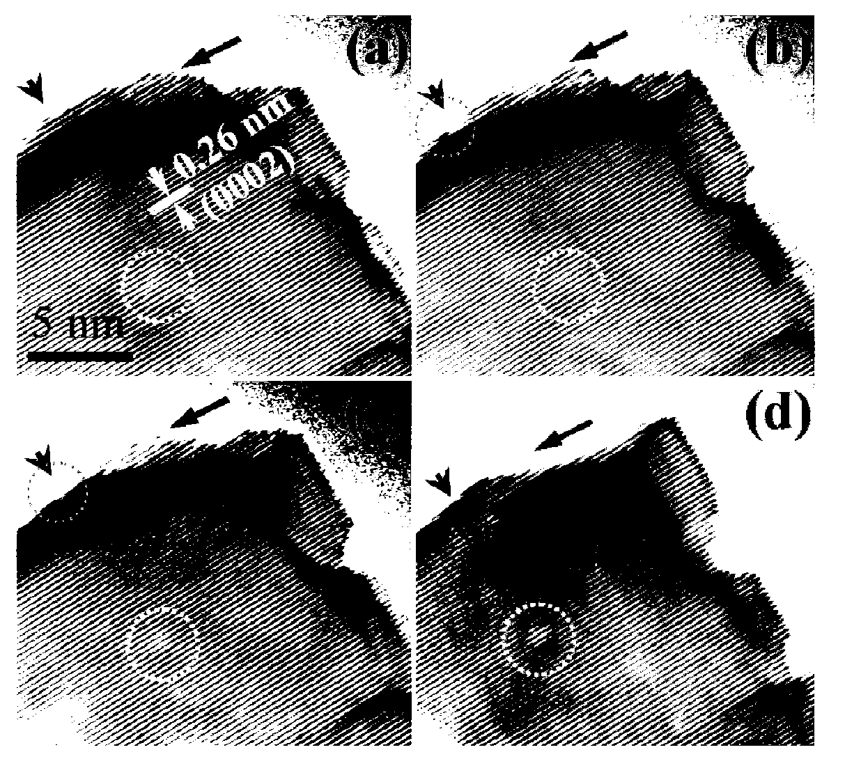
[0028] 4) After the sample is stabilized, turn on the TEM, adjust the intensity and focus position of the electron beam, and scan or focus the electron beam on the surface of the sample according to th...
Embodiment 2
[0034] Embodiment 2: a method for preparing substructures below 10 nanometers on the surface of nanomaterials, the method comprising the following steps:
[0035] 1) Choose zinc oxide nanowires with good crystallization and diameter less than 50 nanometers; the length of zinc oxide nanowires is not limited;
[0036] 2) The nanowires supported by the above-mentioned nanowires are carried on the copper mesh; the copper mesh used is a commercially available copper mesh used for TEM experiments, generally with a diameter of 3 mm and a mesh number of 200-2000 meshes;
[0037] 3) Put the supported nanowires into the electron microscope (TEM) sample rod, then insert it into the vacuum chamber of the TEM, and evacuate until the electron gun can work normally; the vacuum degree of the vacuum chamber is 8.0±1.0×10 -5 Pa;
[0038] 4) Turn on the TEM, adjust the intensity and focusing position of the electron beam, and scan or focus the electron beam on the surface of the sample accordin...
Embodiment 3
[0041] Example 3: It is basically the same as Example 1, the difference is: the nanowires have been prepared into devices, so step 3) can be directly performed, wherein the nanowires are zinc oxide nanowires with good crystallinity and a diameter of less than 50 nanometers .
PUM
| Property | Measurement | Unit |
|---|---|---|
| diameter | aaaaa | aaaaa |
Abstract
Description
Claims
Application Information
 - R&D
- Intellectual Property
- Life Sciences
- Materials
- Tech Scout
- Unparalleled Data Quality
- Higher Quality Content
- 60% Fewer Hallucinations
Browse by: Latest US Patents, China's latest patents, Technical Efficacy Thesaurus, Application Domain, Technology Topic, Popular Technical Reports.
© 2025 PatSnap. All rights reserved.Legal|Privacy policy|Modern Slavery Act Transparency Statement|Sitemap|About US| Contact US: help@patsnap.com