
Non-volatile highly-resistant-single-particle configuration memory unit

A memory cell and single-particle technology, applied in the field of integrated circuits, can solve the problems of non-mentioned, non-volatile memory, and weakened anti-radiation effect of DICE cells, so as to save the external configuration memory and simplify the system.

Inactive Publication Date: 2013-04-03
UNIV OF ELECTRONICS SCI & TECH OF CHINA
View PDF2 Cites 18 Cited by
  • Summary
  • Abstract
  • Description
  • Claims
  • Application Information

AI Technical Summary

Problems solved by technology

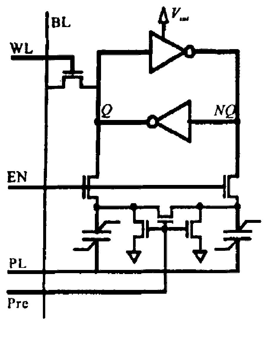
Although this paper proposes an improved DICE SRAM anti-radiation unit, the memory is not non-volatile. At the same time, as the chip processing line width gradually decreases, the anti-radiation effect of the DICE unit will increase with the density of the transistor. increases and weakens, and the article does not mention that this structure can be applied to the field of FPGA

Method used


Image

  • Non-volatile highly-resistant-single-particle configuration memory unit
  • Non-volatile highly-resistant-single-particle configuration memory unit
  • Non-volatile highly-resistant-single-particle configuration memory unit

Examples


Embodiment 1

[0040] Embodiment 1: see Figure 5 .

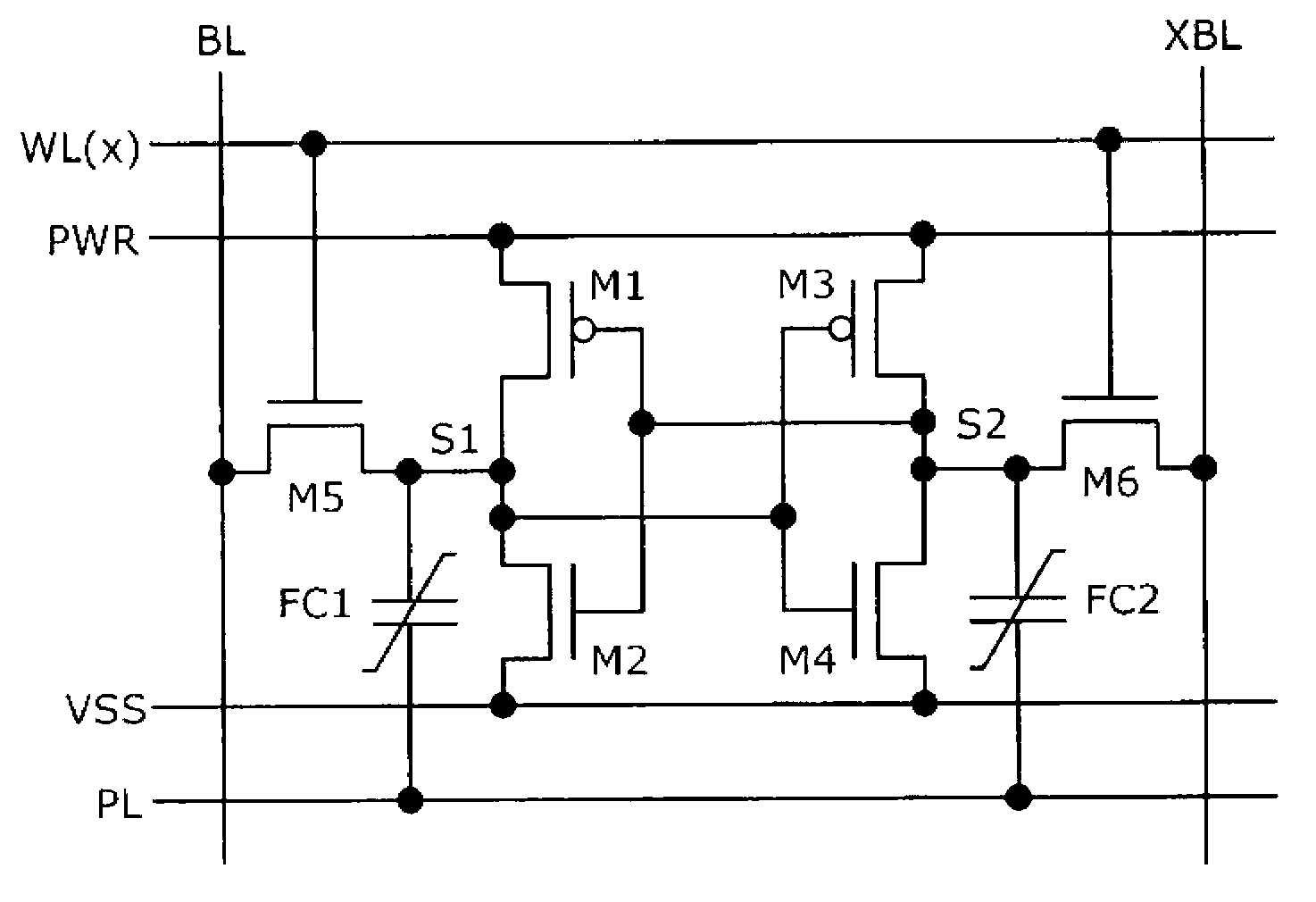
[0041] This embodiment includes 8 MOS transistors, gate MOS transistors and PL board lines that form a 4-level DICE structure. Among the 4 nodes (P1~P4) of the DICE structure, the two nodes marked P1 and P4 are used as ferroelectric A connection node, the ferroelectric connection node refers to a node connected to the PL board line through a ferroelectric capacitor.

[0042] Specifically, this embodiment includes a first ferroelectric capacitor FeC1, a second ferroelectric capacitor FeC2, and 10 MOSFETs (M1~M10), wherein the MOS transistors marked as M1, M3, M5, and M7 are PMOS transistors, marked as The MOS tubes of M2, M4, M5, and M8 are NMOS tubes, which together form an 8-tube DICE SRAM structure. The MOS transistors marked M9 and M10 are the read and write gates controlled by the word line WL signal, VCC and VSS are the high and low power supplies of the chip, BL and ~BL are a pair of opposite bit line signals, and the PL signal is r...

Embodiment 2

[0044] Example 2: see Figure 6 .

[0045] The difference between this embodiment and embodiment 1 is that the connection positions of FeC1 and FeC2 are changed. In Embodiment 1, the two nodes at the front and rear ends are used as ferroelectric connection nodes. In this embodiment, the two nodes in the middle are used as ferroelectric connection nodes, that is, the two nodes marked as P2 and P3 are used as ferroelectric connection nodes.

Embodiment 3

[0046] Embodiment 3: see Figure 7 .

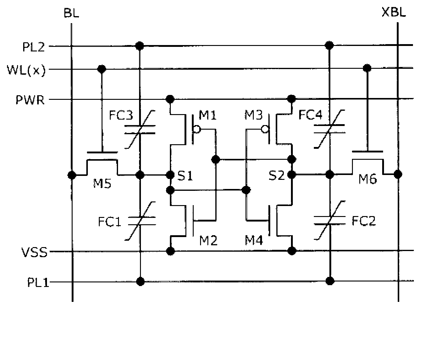
[0047] The difference between this embodiment and Embodiment 1 is that in this embodiment, four ferroelectric capacitors FeC1-FeC4 are respectively connected to the four nodes of the DICE.


PUM


Abstract

The invention discloses a non-volatile highly-resistant-single-particle configuration memory unit and relates to an integrated circuit technique. The configuration memory unit comprises eight MOS (metal oxide semiconductor) transistors, gating MOS transistors and PL (party line) board lines, which form a four-level DICE (dual interlocked storage cell) structure. The configuration memory unit is characterized in that at least two of four nodes in the DICE structure are taken as ferroelectric connection nodes which can be connected to the PL board lines through ferroelectric capacitors. According to the invention, the DICE structure and the ferroelectric capacitors form a non-volatile FPGA (field programmable gate array), therefore, compared with an SRAM (static random access memory) type FPGA, an external configuration memory is eliminated, a system is simplified and the single-particle-resistant capacity of the non-volatile FPGA is substantially increased.

Description

technical field [0001] The present invention relates to integrated circuit technology. Background technique [0002] Electronic systems are more and more widely used in the aerospace field, and the influence of space radiation environment on electronic systems cannot be ignored. Radiation will degrade the performance parameters of the device, and even fail, affecting the reliable operation of the satellite and shortening the life of the satellite. According to satellite data statistics, 70% of its abnormal records are caused by the space radiation environment. With the development of aerospace electronic technology, field programmable gate array (FPGA) has received more and more attention. FPGA combines the advantages of semi-customized gate array circuits with the user-programmable features of programmable logic devices. The designed electronic products have achieved integration, miniaturization, high reliability, and high speed, and provide designers with the ability to ...

Claims


Application Information

Patent Timeline
IPC IPC(8): G11C11/413G11C16/02
Inventor 胡滨李威李平翟亚红刘俊杰刘洋辜科
Owner UNIV OF ELECTRONICS SCI & TECH OF CHINA
Learn More