MIM (metal-insulator-metal) capacitor and manufacturing method thereof

A manufacturing method and technology of capacitors, which are applied in the direction of circuits, electrical components, and electric solid devices, can solve problems such as MIM capacitor short circuit, dielectric layer breakdown, affecting product yield and reliability, etc., to reduce process complexity, The effect of reducing the probability of breakdown and improving reliability

Inactive Publication Date: 2013-04-03
SHANGHAI HUAHONG GRACE SEMICON MFG CORP
View PDF6 Cites 12 Cited by
  • Summary
  • Abstract
  • Description
  • Claims
  • Application Information

AI Technical Summary

Problems solved by technology

As the manufacturing process progresses, due to the existence of the height difference between the upper and lower plates 102 and 101, the via holes will be etched. When the layer 103 is discharged, the potential difference between the upper and lower plates 102 and 101 begins to decrease until the through hole is etched and contacts the lower electrode plate 101. In severe cases, the above discharge process will break down the dielectric layer 103, resulting in a short circuit of the MIM capacitor
The above two problems will seriously affect the performance and reliability of MIM capacitors, especially for some products, the number of MIM capacitors is large, and its area reaches more than 10% of the overall area of ​​the device. Any short circuit or reliability problem of any MIM capacitor will be serious. Affects the yield and reliability of the entire product

Method used


Image

  • MIM (metal-insulator-metal) capacitor and manufacturing method thereof
  • MIM (metal-insulator-metal) capacitor and manufacturing method thereof
  • MIM (metal-insulator-metal) capacitor and manufacturing method thereof

Examples


Embodiment 1

[0035] Figure 2 to Figure 6 Shown is a schematic cross-sectional view of the structure of a method for manufacturing an MIM capacitor. Combine the following Figure 2 to Figure 6 The technical solution of this embodiment will be specifically described.

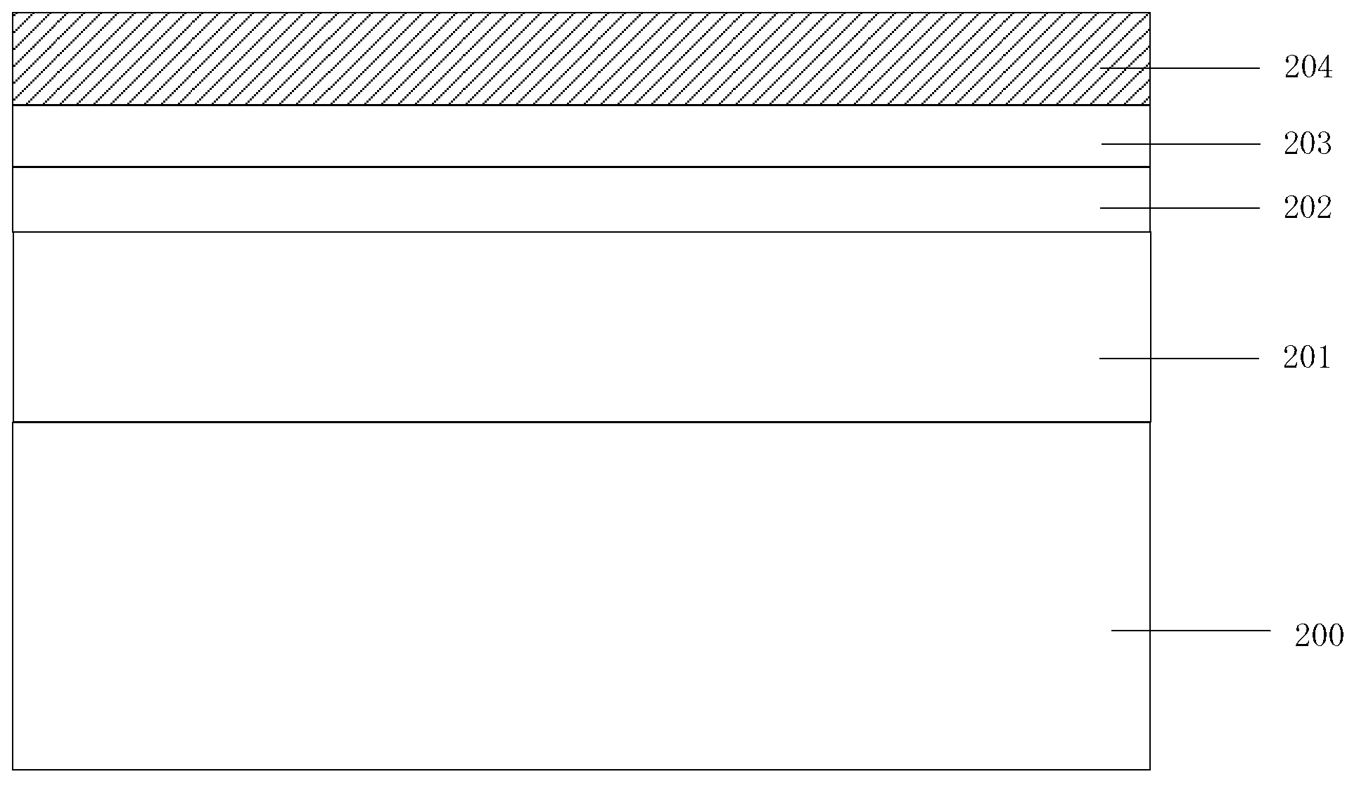
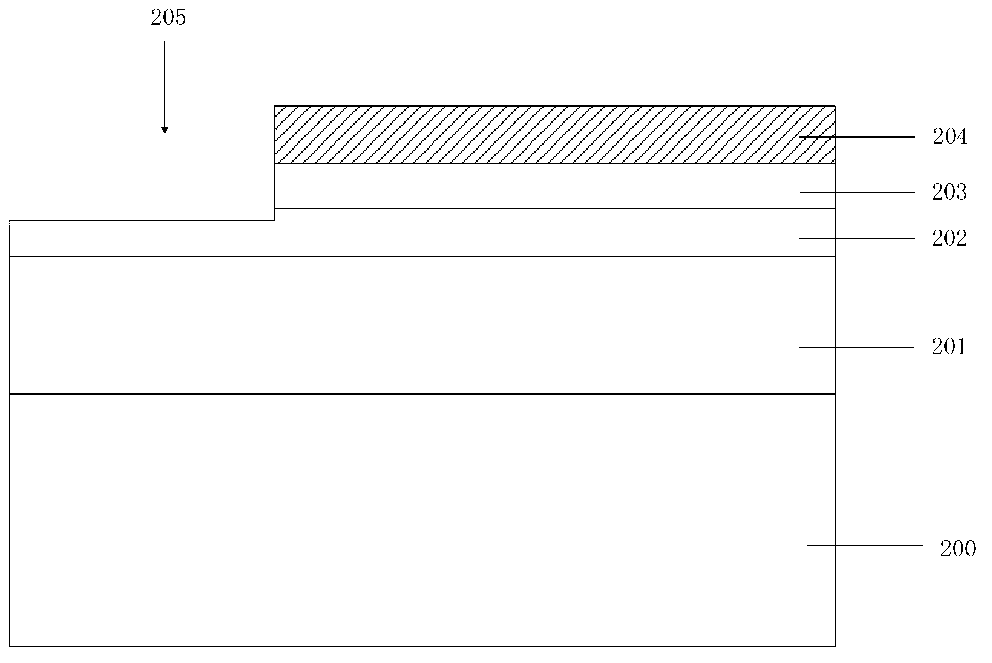
[0036] First, refer to figure 2 As shown, step S11 is performed: a substrate 200 is provided, and a first conductive layer 201 , a capacitor dielectric layer 202 , a second conductive layer 203 and a cover layer 204 are sequentially deposited on the substrate 200 from bottom to top.

[0037] The substrate 200 provided in this step may be a semiconductor substrate on which a premetal dielectric (PMD) is formed, or a semiconductor substrate on which various devices or metal interconnect structures are formed. Conductive layer 201 is electrically insulated from pre-formed various devices or metal interconnect structures.

[0038]The first conductive layer 201 formed in this step is used to form the lower plate of the MIM ca...

Embodiment 2

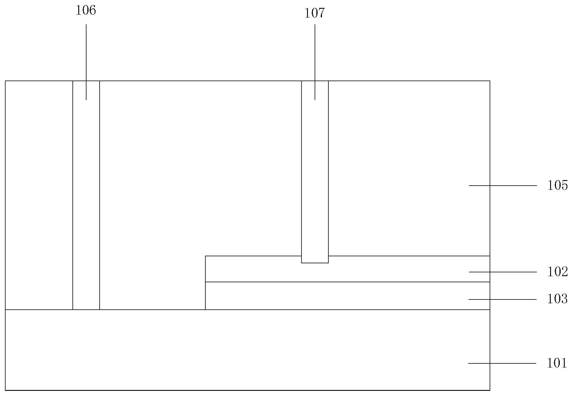
[0054] The structure and fabrication method of the MIM capacitor provided in the second embodiment are substantially the same as those in the first embodiment. The difference lies in: the material and thickness of each layer of the capacitor dielectric layer 202 and the cover layer 204 deposited in step S11, the thickness and material of the dielectric layer 206 formed in step S13, and the dry etching gas selection in step S14, It satisfies that the two through holes 208 and 207 formed by the dry etching in step S13 expose the second conductive layer 203 while exposing the first conductive layer 201 . In other words, the above etching process will not cause damage to the upper electrode plate and the lower electrode plate, and the accumulation degree of positive charges in the upper electrode plate is further reduced, thereby further improving the reliability of the MIM capacitor.

[0055] Specifically, for the case where the capacitor dielectric layer 202 and the cover layer ...


PUM


Abstract

Disclosed are a MIM capacitor and a manufacturing method thereof. The manufacturing method includes: setting a covering layer on a second conducting layer (used for forming an upper electrode plate of an MIM capacitor). Etching gas which is slower in etching the covering layer than etching dielectric layers is selected in the process of dry etching performed to form through holes respectively exposing a first conducting layer (a lower electrode plate) and a second conducting layer, so that excessive etching of the second conducting layer (the upper electrode plate) is avoided when the dielectric layers embedding the second conducting layer and the first conducting layer are etched simultaneously at the same height. Thus, probability of breakdown of the MIM capacitor is lowered, and reliability of the MIM capacitor is increased.

Description

technical field [0001] The invention relates to the field of semiconductor manufacturing, in particular to a MIM capacitor and a manufacturing method thereof. Background technique [0002] Passive devices such as resistors and capacitors are widely used in integrated circuit manufacturing technology. These devices usually use standard integrated circuit technology, using conductive materials such as doped monocrystalline silicon and doped polysilicon, and insulating oxide films or oxynitride films. Made of materials, such as PIP (Poly-Insulator-Poly) capacitors. These devices are relatively close to the silicon substrate, and the parasitic capacitance between the device and the substrate will affect the performance of the device, especially in radio frequency (RF) circuits, as the frequency increases, the performance of the device degrades rapidly. [0003] The proposal of MIM (Metal-Insulator-Metal) capacitor technology provides an effective way to solve this problem. Thi...

Claims


Application Information

Patent Timeline
Patent Type & Authority Applications(China)
IPC IPC(8): H01L21/02H01L23/522
Inventor 黎坡
Owner SHANGHAI HUAHONG GRACE SEMICON MFG CORP
Why Eureka
Try Eureka