Laser annealing device and laser annealing method

A laser annealing and annealing technology, applied in laser welding equipment, electrical components, circuits, etc.

Active Publication Date: 2016-06-29
SUMITOMO HEAVY IND LTD
View PDF8 Cites 0 Cited by
  • Summary
  • Abstract
  • Description
  • Claims
  • Application Information

AI Technical Summary

Problems solved by technology

Since the time to reach the peak is instantaneous, it is difficult to sufficiently heat the deep region of the annealing object

Method used


Image

  • Laser annealing device and laser annealing method
  • Laser annealing device and laser annealing method
  • Laser annealing device and laser annealing method

Examples


Embodiment Construction

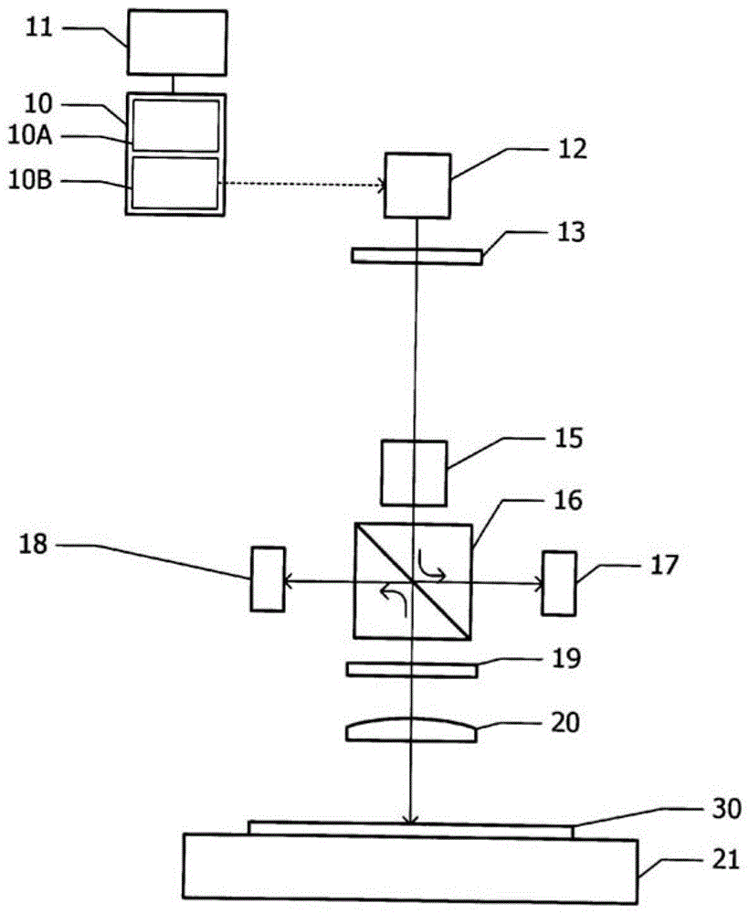
[0026] figure 1 A schematic diagram of a laser annealing apparatus based on an embodiment is shown in . The laser light source 12 is driven by the driver 10 . The laser light source 12 uses, for example, a laser diode with an oscillation wavelength of 690 nm to 950 nm. In this embodiment, a laser diode with an oscillation wavelength of 800 nm is used.

[0027] The laser light source 12 has a plurality of horizontally long light emitting points. The plurality of light emitting points are arranged in a row in the direction of the long sides. The size ratio of the major axis direction and the minor axis direction of each light emitting point is, for example, 100:1. The dimension in the long-axis direction of the light-emitting points is almost equal to the interval between two adjacent light-emitting points. In other words, the luminous points and non-luminous regions are alternately arranged at equal intervals.

[0028] Generally, the spread angle of the laser beam in the ...


PUM

PropertyMeasurementUnit
thicknessaaaaaaaaaa
wavelengthaaaaaaaaaa

Abstract

The invention provides a laser annealing device and a laser annealing method. A general pulse waveform rises sharply from the start of oscillation, shows a peak value, and then gradually decreases. When the power shows a peak value, the surface of the annealing object is rapidly heated to a high temperature. Since the peak time is instantaneous, it is difficult to sufficiently heat the deep region of the annealing object. In the laser annealing apparatus of the present invention, when a pulse current is input, a laser pulse is emitted from a laser diode. The optical system guides the laser beam emitted from the laser diode to the annealing object. The driver supplies a pulse current having a top flat time waveform and a pulse width of 1 μs to 100 μs to the laser diode.

Description

technical field [0001] The invention relates to a laser annealing device and a laser annealing method. Background technique [0002] In the heat treatment of semiconductor wafers, especially silicon wafers, heating in electric furnaces and rapid thermal annealing (RTA) are generally used. The heating time when applying RTA is on the order of milliseconds. In recent years, the application of laser spike annealing with a heating time shorter than 1 μs is also advancing. [0003] In laser spike annealing in which the heating time is shorter than 1 μs, the temperature gradient in the thickness direction of the semiconductor wafer becomes steep due to the short heating time. Therefore, it is difficult to heat the deep region to a desired temperature without excessively raising the surface temperature of the semiconductor wafer. On the other hand, in RTA, since the heating time is long, the temperature of the entire semiconductor wafer rises. Due to the temperature rise of the...

Claims


Application Information

Patent Timeline
Patent Type & Authority Patents(China)
IPC IPC(8): H01L21/268H01L29/739B23K26/073B23K26/0622H01L21/02H01L21/265H01L21/336H01L29/78
CPCB23K26/0732B23K26/0738B23K26/0622B23K2101/40H01L21/268H01L29/7395H01L21/26
Inventor 若林直木万雅史
Owner SUMITOMO HEAVY IND LTD
Why Eureka
Try Eureka