Quantum dot light emitting diode bottom electrode and preparation method thereof

A quantum dot light-emitting and bottom electrode technology, which is applied to circuits, electrical components, and electrical solid devices, can solve problems such as complicated steps, and achieve the effects of avoiding negative effects, improving performance, and reducing manufacturing costs

Pending Publication Date: 2022-06-24
TCL CORPORATION
View PDF0 Cites 0 Cited by
  • Summary
  • Abstract
  • Description
  • Claims
  • Application Information

AI Technical Summary

Problems solved by technology

[0005] The purpose of the present invention is to provide a bottom electrode of a quantum dot light-emitting diode and a preparation method thereof, aiming at solving the problem of complicated steps in the wet etching preparation process of the bottom electrode of an existing top-emitting quantum dot light-emitting diode

Method used


Image

  • Quantum dot light emitting diode bottom electrode and preparation method thereof
  • Quantum dot light emitting diode bottom electrode and preparation method thereof
  • Quantum dot light emitting diode bottom electrode and preparation method thereof

Examples


preparation example Construction

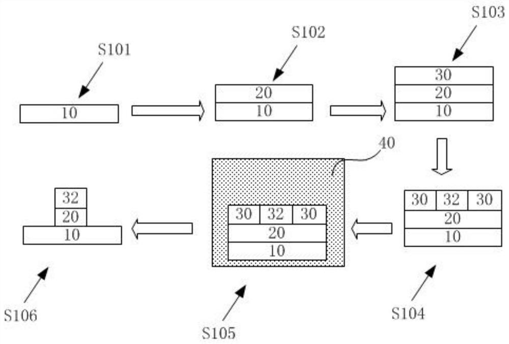
[0024] An embodiment of the present invention provides a method for preparing a bottom electrode of a quantum dot light-emitting diode, which includes the following steps:

[0025] S1. Provide a substrate, and prepare a reflective layer on the surface of the substrate;

[0026] S2, preparing an electrode layer on the surface of the reflective layer away from the substrate, and performing crystallization treatment and etching treatment on the electrode layer to obtain a bottom electrode of a quantum dot light-emitting diode.

[0027] In the method for preparing the bottom electrode of a quantum dot light-emitting diode provided by the embodiment of the present invention, firstly, the electrode layer can be crystallized by crystallizing the electrode layer, which is originally in an amorphous state, and then the conductive metal oxide in the electrode layer can be crystallized. Etching removes the uncrystallized part, which not only achieves the purpose of full annealing, improv...
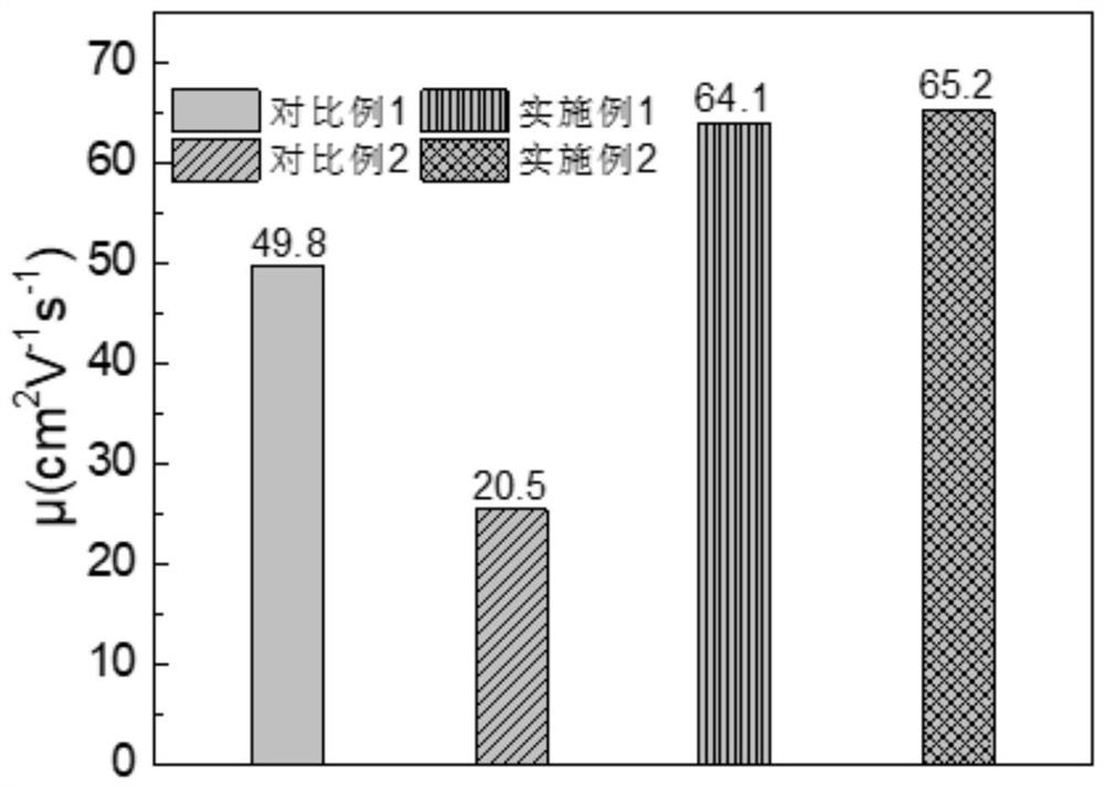
Embodiment 1

[0060] A method for preparing a bottom electrode of a top emission quantum dot light-emitting diode, comprising the following steps:

[0061] (11) Provide blank glass substrate;

[0062] (12) On a blank glass substrate, through thermal evaporation, the vacuum degree is not higher than 3×10 -4 Pa, Ag was evaporated, the speed was 1 angstrom / second, and the time was 1000 seconds to obtain a reflective layer with a thickness of 100 nm;

[0063] (13) Spin coating the ITO precursor solution, rotating speed 3000, time 30 seconds, using electron beam to scan the film 10 -2 Second, the film is thermally annealed, and this process is repeated ten times with an interval of 2 s each time to crystallize the ITO film layer. Wherein, the area of ​​annealing is the desired shape of the ITO electrode layer. The accelerating voltage of the electron beam is 10 2 kV, the energy density of the electron beam is 0.825J / cm 2 , after annealing, let it cool for 5 minutes;

[0064] (14) preparing...

Embodiment 2

[0068] A method for preparing a bottom electrode of a top emission quantum dot light-emitting diode, comprising the following steps:

[0069] (21) Provide blank glass substrate;

[0070] (22) On a blank glass substrate, through thermal evaporation, the degree of vacuum is not higher than 3×10 -4 Pa, Ag was evaporated, the speed was 1 angstrom / second, and the time was 1000 seconds to obtain a reflective layer with a thickness of 100 nm;

[0071] (23) Spin-coating ITO precursor solution, rotating speed 3000, time 30 seconds, using femtosecond laser irradiation for 10 seconds -2 Second, the film is thermally annealed, and this process is repeated ten times with an interval of 2 s each time to crystallize the ITO film layer. Wherein, the area of ​​annealing is the desired shape of the ITO electrode layer. The laser beam diameter is 3mm, the wavelength is 1053nm, the pulse width is 120fs, the repetition frequency is 1kHz, and the beam quality factor is 1.2. After annealing, it w...


PUM

PropertyMeasurementUnit
thicknessaaaaaaaaaa
thicknessaaaaaaaaaa
diameteraaaaaaaaaa

Abstract

The invention relates to the technical field of display, and provides a quantum dot light emitting diode bottom electrode and a preparation method thereof. According to the invention, the electrode layer is crystallized, so that the conductive metal oxide which is originally in an amorphous state in the electrode layer can be crystallized, and then the non-crystallized part is removed through etching treatment, so that the purpose of full annealing can be achieved, and the carrier mobility of the electrode layer is improved; and the negative influence on the reflecting layer in the conventional heating and annealing treatment process is avoided. Meanwhile, laser etching equipment is not needed in the preparation process, a resist film layer does not need to be prepared either, the preparation technology is simplified, the production cost is reduced, and the method is more suitable for the requirement for small-scale research and development in a laboratory. The bottom electrode of the quantum dot light-emitting diode is used for preparing a top-emitting quantum dot light-emitting diode, and the obtained top-emitting quantum dot light-emitting diode has good light-emitting efficiency and performance.

Description

technical field [0001] The invention belongs to the technical field of display, and in particular relates to a bottom electrode of a quantum dot light-emitting diode and a preparation method thereof. Background technique [0002] Quantum Dots Light-Emitting Diode (QLED) is an emerging display device whose structure is similar to that of an organic light-emitting display (Organic Light-Emitting Diode, OLED). A sandwich structure composed of electron transport layers. This is a new technology between liquid crystal and OLED, and its core technology is "Quantum Dot". As early as 1983, scientists from Bell Labs in the United States conducted in-depth research on it, and a few years later, physicist Mark Reed of Yale University in the United States officially named it "quantum dots". Quantum dots are particles with a particle diameter of less than 10 nm, composed of zinc, cadmium, sulfur, and selenium atoms. This substance has a very special property: when quantum dots are sti...

Claims


Application Information

Patent Timeline
Patent Type & Authority Applications(China)
IPC IPC(8): H01L51/52H01L51/50H01L51/56
CPCH10K50/115H10K50/805H10K71/00
Inventor 敖资通严怡然张建新杨帆赖学森洪佳婷
Owner TCL CORPORATION
Why Eureka
Try Eureka