

Light-emitting diode (LED) epitaxial structure with quaternary InAlGaN and method for preparing same
An epitaxial structure, n-type technology, applied in electrical components, gaseous chemical plating, coating, etc., can solve problems such as separation and quantum efficiency reduction
- Summary
- Abstract
- Description
- Claims
- Application Information
AI Technical Summary
Problems solved by technology
Method used
Image

Examples
Embodiment 1
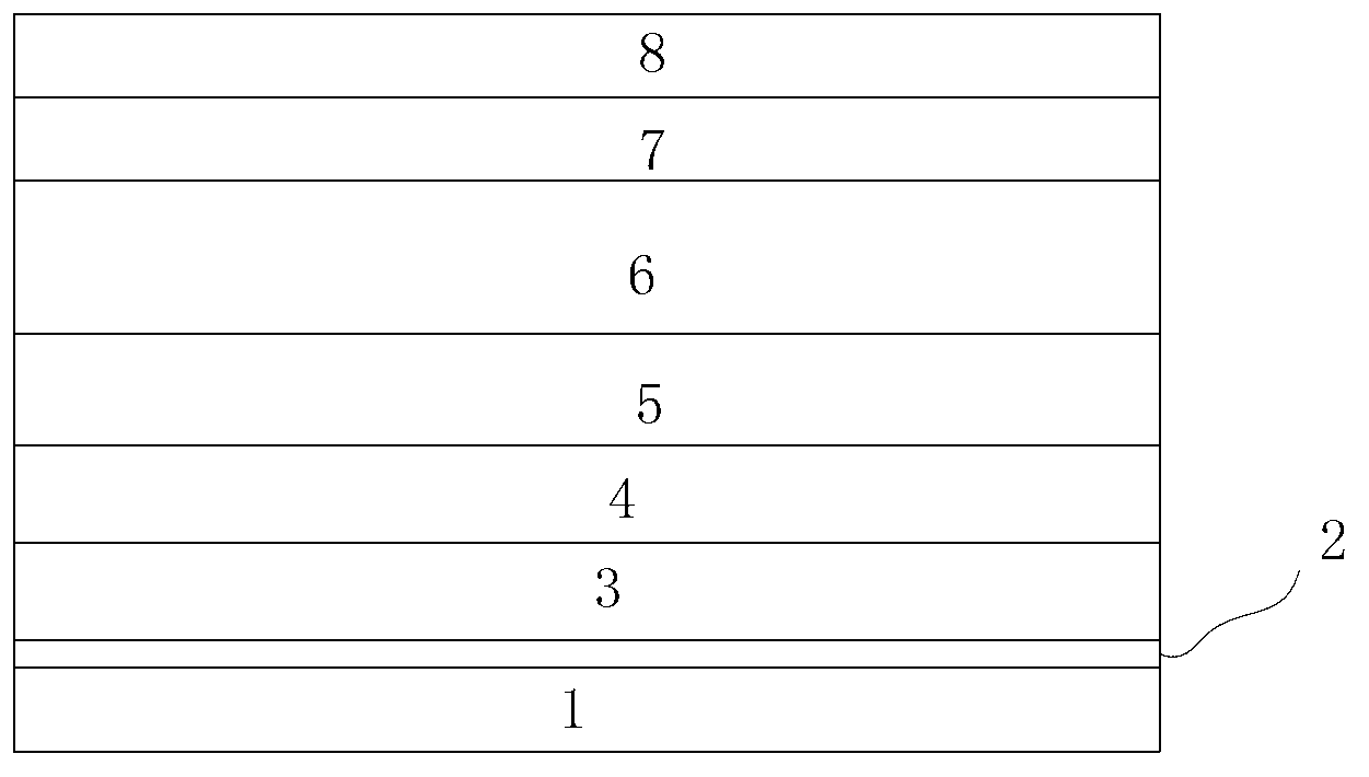
[0066] see figure 1 , the LED epitaxial structure with quaternary InAlGaN of the present invention includes: a substrate 1, on the substrate 1, a GaN buffer layer 2, an undoped GaN layer 3, and an n-type doped GaN layer are sequentially arranged from bottom to top 4. InAlGaN stress release layer 5 , multiple quantum well light emitting layer 6 , p-type doped InAlGaN electron blocking layer 7 and p-type doped GaN layer 8 .
[0067] Among them, the thickness of the GaN buffer layer 2 is 25nm; the thickness of the undoped GaN layer 3 is 2.2μm; the thickness of the n-type doped GaN layer 4 is 2.3μm; the thickness of the InAlGaN stress release layer 5 is 50nm; The thickness of well light-emitting layer 6 is 240nm; the thickness of p-type doped InAlGaN electron blocking layer 7 is 50nm; the thickness of p-type doped GaN layer 8 is 250nm.
[0068] The above-mentioned LED epitaxial structure is prepared by the following preparation method of the LED epitaxial structure, and the prepa...
Embodiment 2
[0091] see Figure 4 , the LED epitaxial structure with quaternary InAlGaN of the present invention includes: a substrate 1, on the substrate 1, a GaN buffer layer 2, an undoped GaN layer 3, and an n-type doped GaN layer are sequentially arranged from bottom to top 4. Undoped GaN quantum well barrier layer 9, InAlGaN stress release layer 5, multiple quantum well light emitting layer 6, p-type doped InAlGaN electron blocking layer 7 and p-type doped GaN layer 8.
[0092] Wherein, the thickness of GaN buffer layer 2 is 20nm; The thickness of undoped GaN layer 3 is 2 μm; The thickness of n-type doped GaN layer 4 is 2 μm; The thickness of the quantum well barrier layer 9 of undoped GaN is 2.5 μm; the thickness of the InAlGaN stress release layer 5 is 40nm; the thickness of the multi-quantum well light-emitting layer 6 is 245nm; the thickness of the p-type doped InAlGaN electron blocking layer 7 is 60nm; the thickness of the p-type doped GaN layer 8 is 200nm.
[0093] The above-m...
PUM
| Property | Measurement | Unit |
|---|---|---|
| Thickness | aaaaa | aaaaa |
| Thickness | aaaaa | aaaaa |
| Thickness | aaaaa | aaaaa |
Abstract
Description
Claims
Application Information