Vertical transition from broadband micro strip to micro strip

A vertical transition and microstrip technology, applied in the direction of electrical components, connecting devices, circuits, etc., can solve the problems of high processing precision, increase processing cost, limit bandwidth, etc., achieve convenient processing and production, reduce production cost, and increase bandwidth Effect

Active Publication Date: 2013-04-03
BEIJING RES INST OF TELEMETRY +1
View PDF2 Cites 8 Cited by
  • Summary
  • Abstract
  • Description
  • Claims
  • Application Information

AI Technical Summary

Problems solved by technology

The disadvantage of this method is: this structure can be equivalent to a low-pass circuit, especially the parasitic mode generated by the discontinuity at high frequency makes the electromagnetic wave resonate, which limits the bandwidth of this structure, and the hole structure has a great impact on the processing accuracy. Higher requirements, increased processing costs
[0004] In broadband microwave and millimeter wave systems, the current microstrip to microstrip vertical transition technology still cannot better meet the requirements of the application, so its application is subject to certain restrictions

Method used


Image

  • Vertical transition from broadband micro strip to micro strip
  • Vertical transition from broadband micro strip to micro strip
  • Vertical transition from broadband micro strip to micro strip

Examples


Embodiment 1

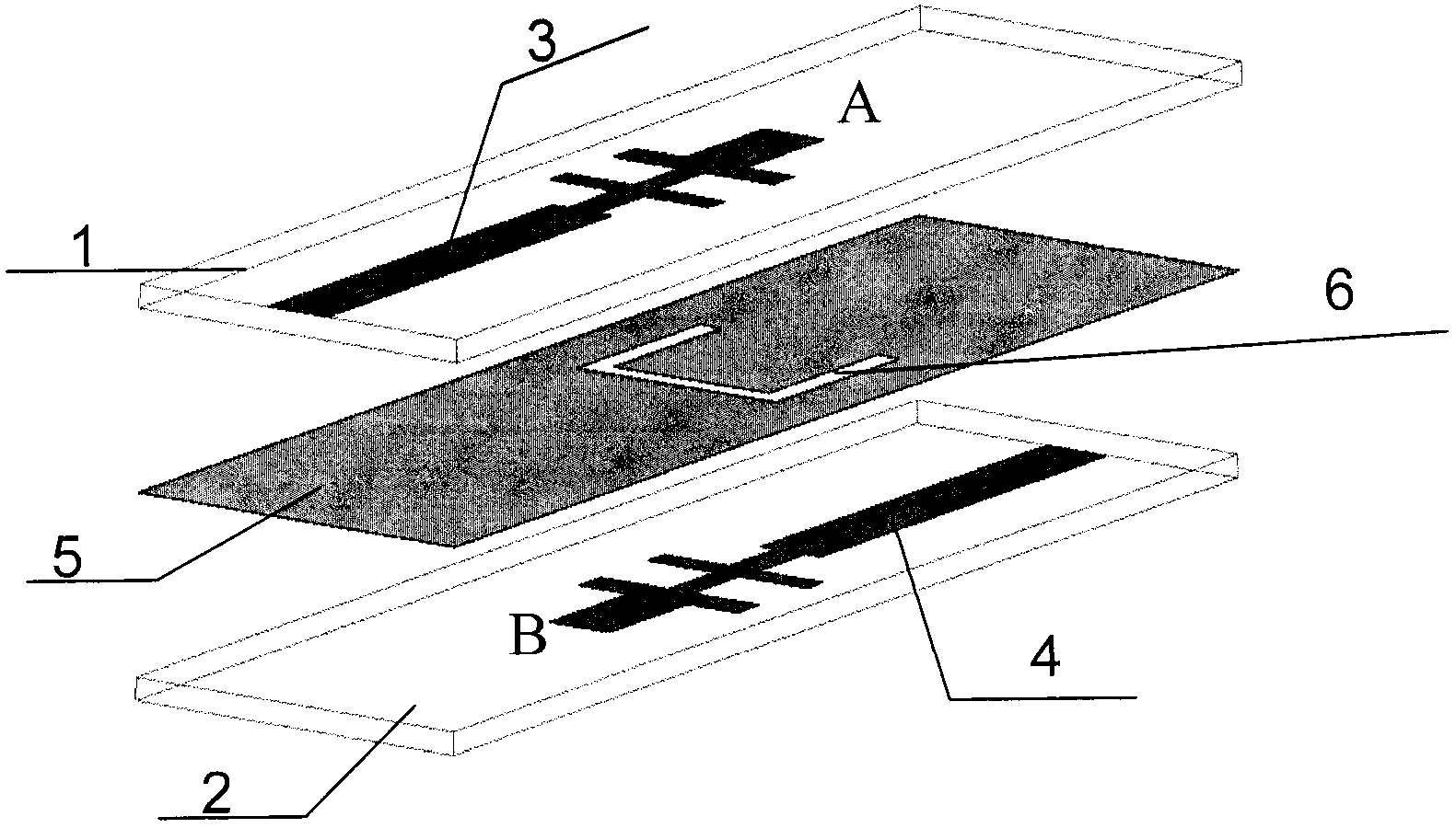
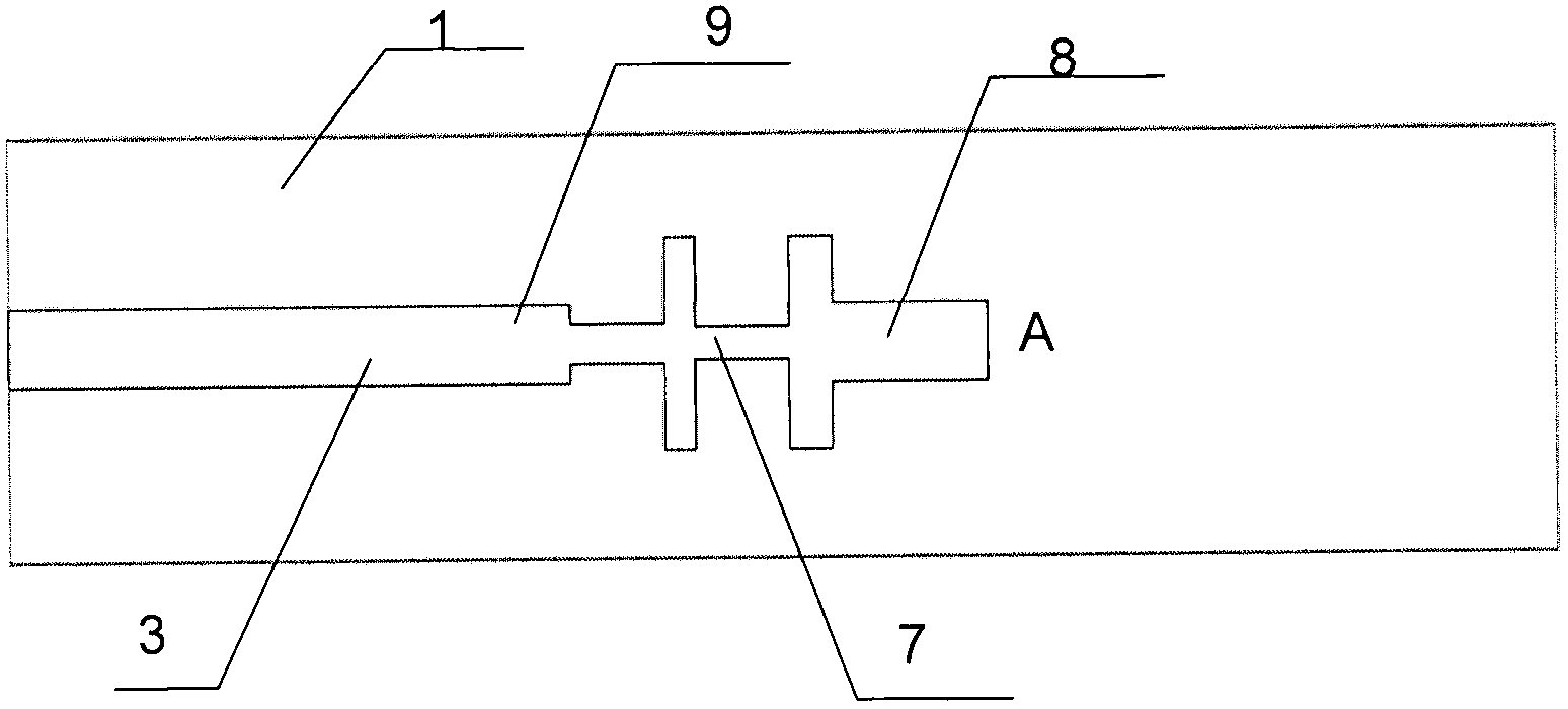
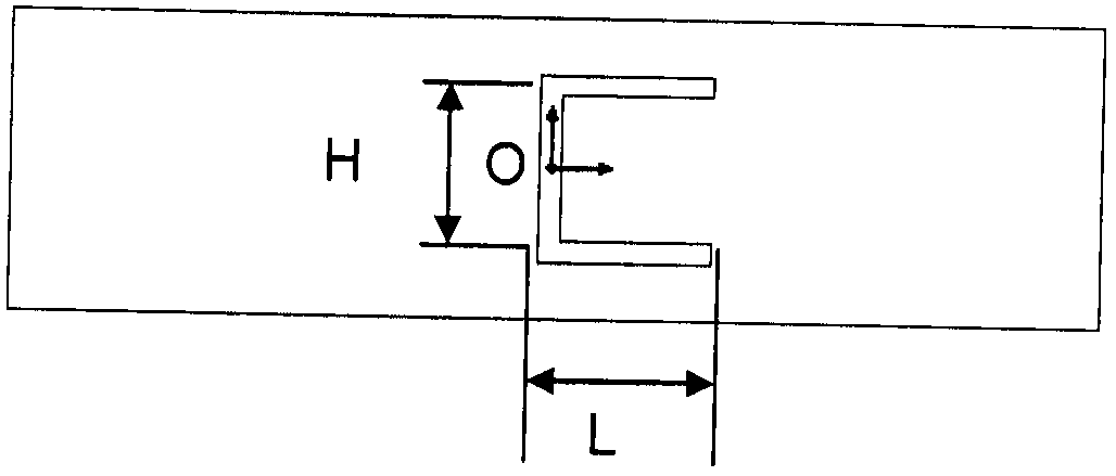
[0037] The vertical transition structure adopts two layers of Rogers5880 substrates 1 and 2 with a dielectric constant of 2.2, and the thickness of each layer is 0.508mm. The middle ground layer 5 is a metal copper layer with a U-shaped groove 6. The microstrip line structures 3 and 4 are composed of 50 ohm microstrip lines 8 and 9 and two-order open-circuit high and low impedance stubs 7. The structure is optimized by electromagnetic simulation. The specific dimensions are:

[0038] (1) The length of the first dielectric substrate 1 is 24mm, the width is 8mm, and the height is 0.508mm;

[0039] (2) The length of the second dielectric substrate 2 is 24mm, the width is 8mm, and the height is 0.508mm;

[0040] (3) The total length of the top microstrip line structure 3 is 18.35mm and the thickness is 17um;

[0041] (4) The total length of the bottom microstrip line structure 4 is 18.35mm and the thickness is 17um;

[0042] (5) The length of the intermediate formation 5 is 24m...


PUM


Abstract

The invention relates to a vertical transition from a broadband micro strip to a micro strip. The vertical transition is composed of a first medium substrate, a middle stratum and a second medium substrate which are parallely distributed, wherein a top layer micro strip structure is arranged at one end of the first medium substrate, a bottom layer micro strip structure is arranged at the other end of the second medium substrate, the top layer micro strip structure is completely same with the bottom layer micro strip structure, the top layer micro strip structure and the bottom layer micro strip structure are oppositely distributed, the middle stratum is a metal layer provided with a U-shaped coupling groove, the top layer micro strip structure and the bottom layer micro strip structure both comprises a first micro strip line, a second micro strip line and a high-low impedance stub line of a two-stage terminal open circuit, and the high-low impedance stub line of the two-stage terminal open circuit is located between the first micro strip line and the second micro strip line. The vertical transition is simple in structure, greatly expands bandwidth, reduces system loss, enables design to be flexible, reduces cost and is wide in applicable scope.

Description

technical field [0001] The invention relates to a vertical transition structure of broadband microstrip to microstrip, which is suitable for three-dimensional interconnection of radio frequency circuit multi-layer technology, especially vertical interconnection of three-dimensional microwave and millimeter-wave integrated circuits, and belongs to the technical field of microwave and millimeter-wave communication. Background technique [0002] With the wide application of wireless communication systems in the microwave and millimeter-wave frequency bands, military electronic systems have smaller and smaller requirements for volume and weight, and the need for high integration is becoming more and more severe. Three-dimensional integrated circuits are a main means to realize the miniaturization of microwave and millimeter-wave circuits. and trends. The 3D integrated microwave circuit is a microwave circuit with a 3D three-dimensional structure based on the 2D MMCM, which makes...

Claims


Application Information

Patent Timeline
Patent Type & Authority Applications(China)
IPC IPC(8): H01P5/00
Inventor 李翠霞祝大龙刘德喜
Owner BEIJING RES INST OF TELEMETRY
Why Eureka
Try Eureka