Unlock instant, AI-driven research and patent intelligence for your innovation.

Fabrication method of flash memory cell structure

The technology of a flash memory unit and its manufacturing method is applied in the field of manufacturing the flash memory unit structure, and can solve the problems affecting the persistence of information stored in the flash memory unit and the shortened service life of the flash memory device, etc.

Active Publication Date: 2015-12-02
CSMC TECH FAB2 CO LTD
View PDF3 Cites 0 Cited by
  • Summary
  • Abstract
  • Description
  • Claims
  • Application Information

AI Technical Summary

Problems solved by technology

When the quality of the insulating layer covering the sidewall of the stacked structure in the flash memory unit is insufficient, it will directly affect the durability of the information stored in the entire flash memory unit, shortening the service life of the entire flash memory device

Method used


Image

  • Fabrication method of flash memory cell structure
  • Fabrication method of flash memory cell structure
  • Fabrication method of flash memory cell structure

Examples


Embodiment Construction

[0018] In order to make the information stored in the flash memory cell structure have good durability and improve the service life of the flash memory cell structure, a flash memory cell structure and a manufacturing method thereof are proposed.

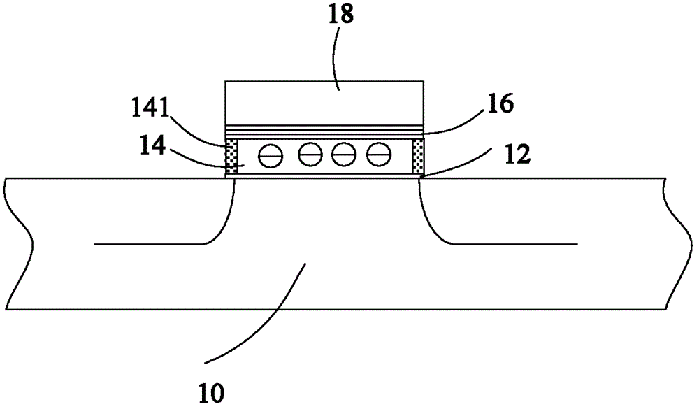
[0019] An example of this flash memory cell structure is figure 1 As shown, it includes a semiconductor base layer 10 and a tunnel oxide layer 12 , a floating gate 14 , an insulating dielectric layer 16 and a control gate 18 sequentially stacked on the semiconductor base layer 10 . A sidewall surface of the floating gate 14 is implanted with an ion-blocking layer 141 .

[0020] When the floating gate 14 is in the state of retaining carriers, the blocking ion layer 141 can effectively increase the barrier height for carriers to escape from the floating gate 14, thereby improving the durability and service life of the flash cell structure storing information.

[0021] In the embodiment of the flash memory cell structure, in order to ...


PUM


Abstract

A flash memory unit structure comprises a semiconductor substrate. A tunneling oxide layer, a floating gate, an insulating medium layer and a control gate are stacked on the semiconductor substrate in sequence. A checking ion sheath is embedded in the surface of a side wall of the floating gate. The manufacture method of the flash memory unit structure includes the following steps: arranging the tunneling oxide layer and the floating gate on the semiconductor substrate in sequence, arranging the insulating medium layer and the control gate on the floating gate, and embedding checking ions in the side wall of the floating gate to form a checking ion layer of the surface of the side wall of the floating gate. When the floating gate is in a state of keeping charge carriers, the checking ion layer of the side wall of the floating gate increases barrier height of the charge carriers to escape from the floating gate, and thereby durability of the flash memory unit structure for saving information is improved and service life of the flash memory unit structure is prolonged.

Description

【Technical field】 [0001] The invention relates to a semiconductor device structure and a manufacturing method, in particular to a flash memory unit structure and a manufacturing method. 【Background technique】 [0002] Flash memory is a common storage device on the market. Flash memory is a type of programmable read-only memory (PROM) relative to read-only memory (ROM). Flash memory cells in flash memory can retain their stored information for up to ten years without being powered on. [0003] A traditional flash memory cell structure includes a semiconductor base layer, a gate dielectric layer stacked on the semiconductor base layer, a floating gate for storing information, an insulating dielectric layer and a control gate. The flash memory unit recognizes digital information such as "0" or "1" by whether there are stored electrons in the floating gate. In order to improve the ability of the flash memory unit to hold information, the sidewall of the stacked structure part...

Claims


Application Information

Patent Timeline
Patent Type & Authority Patents(China)
IPC IPC(8): H01L27/115H01L21/8247H01L29/423G11C16/04H10B69/00
Inventor 王军周玮蔡建祥许宗能
Owner CSMC TECH FAB2 CO LTD