An Optical Sensing System Based on CMOS Processing Technology

A processing technology and optical sensing technology, applied in the field of optical sensing and optical communication, to achieve the effect of extended function application and simple process design

Active Publication Date: 2015-08-12
KUANG CHI INST OF ADVANCED TECH
View PDF4 Cites 0 Cited by
  • Summary
  • Abstract
  • Description
  • Claims
  • Application Information

AI Technical Summary

Problems solved by technology

However, it is difficult for existing optical sensors to simultaneously integrate complex optoelectronic properties into a single chip to simultaneously detect optical signal intensity information and angle information.

Method used


Image

  • An Optical Sensing System Based on CMOS Processing Technology
  • An Optical Sensing System Based on CMOS Processing Technology
  • An Optical Sensing System Based on CMOS Processing Technology

Examples


Embodiment 1

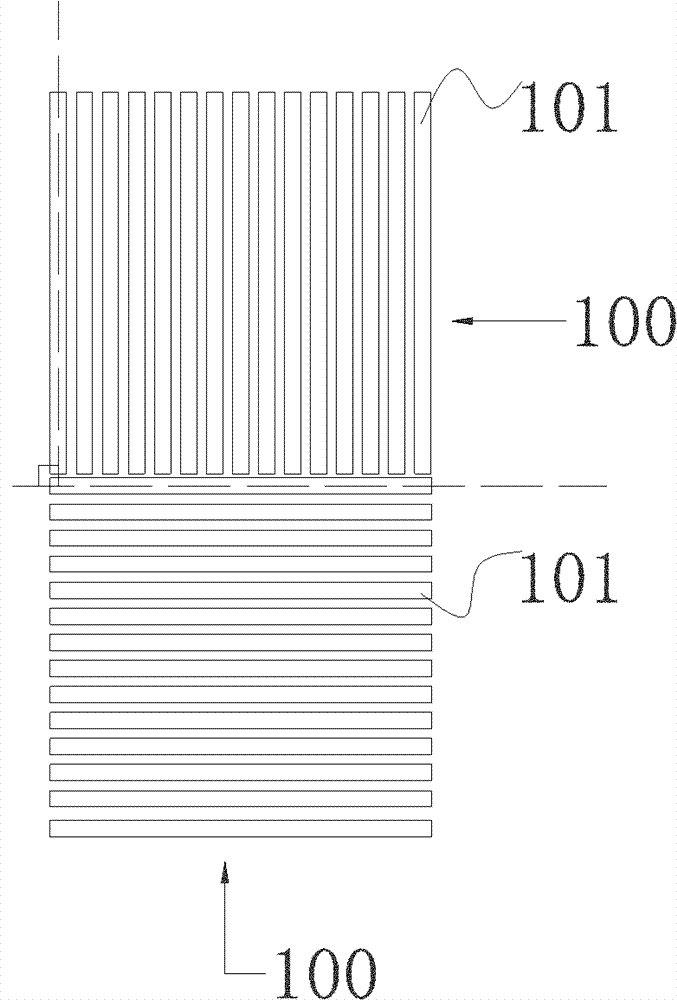
[0021] attached image 3 A schematic diagram of the structure of the sensing unit based on the CMOS process in Embodiment 1 is shown. The sensing unit 100 is composed of a diffraction grating 101, an analysis grating 102 and a PN junction array 103. The diffraction grating 101 and the analysis grating 102 are arranged in a double-layer parallel structure on the CMOS In the metal wiring layer of the circuit board, the analysis grating 102 is arranged in parallel below the diffraction grating 101, and the parallel distance between the analysis grating 102 and the diffraction grating 101 is 1 / 2 times the Tebao distance of the diffraction grating, and four PN junctions form a PN junction The array 103 is located below the analysis grating 102 and is arranged in the silicon substrate layer 200 of the CMOS circuit board. Corresponding to each PN junction, the width of a blocking grating 104 is increased by 1 / 4D in the analysis grating 102 at equal intervals, and D is diffraction The...

Embodiment 2

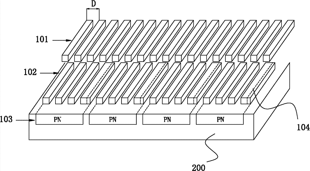
[0033] attached Figure 4A schematic diagram of the structure of the sensing unit based on the CMOS process in Embodiment 2 is shown. The sensing unit 100 is composed of a diffraction grating 101, an analysis grating 102 and a PN junction array 103, and the diffraction grating 101 and the analysis grating 102 are arranged in a double-layer parallel structure In the metal wiring layer of the CMOS circuit board, the analysis grating 102 is arranged in parallel below the diffraction grating 101, the parallel distance between the analysis grating 102 and the diffraction grating 101 is the diffraction grating Taibao distance, and four PN junctions form a PN junction array 103 Located below the analysis grating 102 and arranged in the silicon substrate layer 200 of the CMOS circuit board, corresponding to each PN junction, the width of a grating gap 105 in the analysis grating 102 is increased by 1 / 4D at equal intervals, and D is the diffraction grating 101 The grating pitch is form...


PUM


Abstract

The invention provides an optical sensing system based on a complementary metal-oxide-semiconductor (CMOS) processing technique. The optical sensing system comprises a photo sensor integrally arranged on a CMOS circuit board and an operational circuit connected with the photo sensor, the photo sensor is formed by sensing units in an array, each sensing unit comprises a diffraction grating, an analytical grating and a PN junction array, a perpendicular distance between the analytical grating and the diffraction grating is m / n times of a taibao distance of the diffraction grating, the m and the n are both positive integers, dislocation shielding is formed by the analytical grating on the diffraction grating in certain distance, accordingly detection of angle information of plane light can be conveniently achieved, functional application of light sensing systems is expanded, and the optical sensing system is simple in process design and applicable to large-scale industrialization manufacture.

Description

【Technical field】 [0001] The invention relates to the fields of optical sensing and optical communication, in particular to an optical sensing system based on CMOS processing technology. 【Background technique】 [0002] In the past 30 years, the semiconductor industry has been developing continuously following Moore's Law. As one of the foundations of the semiconductor industry, the semiconductor process technology is also developing and improving day by day. Since the invention of CMOS devices in the mid-1960s, CMOS technology has begun to develop rapidly. CMOS technology is developed on the basis of PMOS and NMOS technology, and NMOS devices and PMOS devices are arranged on the same silicon substrate at the same time. For the production of CMOS integrated circuits, the most basic CMOS processes include: the silicon wafer process for producing the required type of substrate; the photolithography process for determining the processing area; the oxidation, deposition, diffusio...

Claims


Application Information

Patent Timeline
Patent Type & Authority Patents(China)
IPC IPC(8): H01L27/146G01J1/42
Inventor 刘若鹏孙豪文栾琳赵治亚
Owner KUANG CHI INST OF ADVANCED TECH
Why Eureka
Try Eureka