Plane type semiconductor thermoelectric chip and production method thereof

A semiconductor, planar technology, applied in the manufacture/processing of thermoelectric devices, thermoelectric devices that only use the Peltier or Seebeck effect, etc., can solve the problem of small temperature difference between the two ends of the thermocouple, few pairs of thermocouples, cold end and hot end There are no problems such as complete isolation, so as to achieve the effect of increasing the number of thermocouple pairs, good temperature distribution characteristics, and good process compatibility

Active Publication Date: 2013-04-10
SHANGHAI INST OF MICROSYSTEM & INFORMATION TECH CHINESE ACAD OF SCI
View PDF4 Cites 8 Cited by
  • Summary
  • Abstract
  • Description
  • Claims
  • Application Information

AI Technical Summary

Problems solved by technology

[0012] In view of the shortcomings of the prior art described above, the purpose of the present invention is to provide a planar semiconductor thermoelectric chip and its preparation method, which is used to solve the problem that the number of thermocouple pairs in the prior art is small, and the cold end and the hot end are not completely isolated. , the problem of smaller temperature difference across the thermocouple, resulting in higher output voltage and thermoelectric efficiency

Method used


Image

  • Plane type semiconductor thermoelectric chip and production method thereof
  • Plane type semiconductor thermoelectric chip and production method thereof
  • Plane type semiconductor thermoelectric chip and production method thereof

Examples


Embodiment 1

[0091] The thermocouple material is P-type polysilicon and N-type polysilicon, the support layer is Pyrex7740 heat-resistant glass, and the bonding method is silicon-glass anode bonding.

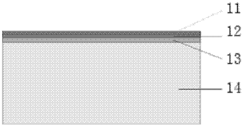
[0092] 1) Take (100) silicon wafer 14 (monocrystalline silicon), and grow silicon oxide 13, silicon nitride 12, and polysilicon film (11) on the front side of the silicon wafer by thermal oxidation and twice LPCVD. See Figure 2-1 .

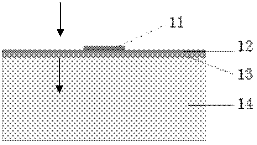
[0093] 2) Perform P-type and N-type ion doping on polysilicon, and dry etching to form two types of resistors, P and N. See Figure 2-2 .

[0094] 3) Aluminum 15 is sputtered and alloyed after wet etching to form an aluminum electrode to realize the electrical connection of the thermocouple pair. See Figure 2-3 .

[0095] 4) Dry etching of silicon nitride and silicon oxide to expose the silicon substrate and reserve a bonding area. See Figure 2-4 .

[0096] 5) Take a Pyrex7740 glass sheet 16, perform isotropic wet etching on the surface, and perform ...

Embodiment 2

[0105] The thermocouple material is polysilicon and metal aluminum, and its specific implementation steps are basically the same as in Example 1. The main difference is that in step 2, the polysilicon film is ion-doped once to make it conductive, and in step 3, aluminum is patterned to form electrodes. Corresponding thermocouples are also formed, paired with polysilicon resistors to form thermocouple pairs, and the rest remain unchanged.

Embodiment 3

[0107] The lower support layer is added to the structure of Example 1. The specific implementation steps are basically the same as in Example 1. After step 6, a bonding process is added to realize bonding with the lower heat-insulating support layer. The material of the support layer is Pyrex7740 heat-resistant glass. See Figure 4 .

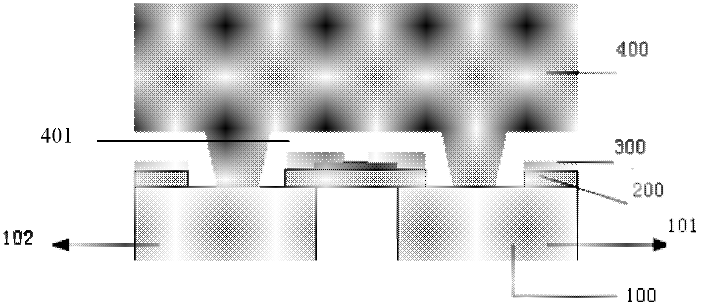
[0108] The present invention proposes a planar thermoelectric chip structure and a manufacturing method. The thermoelectric chip structure includes four parts: a heat conduction layer, an electrical insulation layer, a power generation layer, and a support layer. On the support layer, the middle part of the heat conduction layer is made into a comb-tooth structure, and an electrical insulating layer is made on the surface. The leads are connected to form the power generation layer, such as figure 1 , as shown in Figure 2.

[0109]Compared with the traditional planar thermoelectric chip, the design of this comb-shaped heat-conducting layer str...


PUM

PropertyMeasurementUnit
Spacingaaaaaaaaaa

Abstract

The invention relates to a plane type semiconductor thermoelectric chip and a production method thereof. The production method includes that a silicon slice including a heat conduction layer (100) with two ends completely separated, an insulation layer (200) located on the heat conduction layer and a power generation layer (300) located on the insulation layer is produced, wherein the power generation layer comprises thermocouple pairs (302) and a metal lead and electrode (301) used for connecting the thermocouple pairs; a supporting layer (400) provided with a concave portion and made of heat insulation materials is produced; the supporting layer (400) is bonded with the silicon slice, and the back surface of the silicon slice after bonding is thinned and polished; and the thermocouple pairs (302) are released, and the two ends of the heat conduction layer are bridged through the thermocouple pairs. According to the plane type semiconductor thermoelectric chip and the production method thereof, the quantity of the thermocouple pairs arranged in the single plane type semiconductor thermoelectric chip and the temperature difference utilization rate are greatly improved, and accordingly high voltage and large-power output of the plane type semiconductor thermoelectric chip are achieved. The plane type semiconductor thermoelectric chip and the production method thereof are simple in process and low in cost, can achieve batch production and have the application prospect.

Description

technical field [0001] The invention provides a planar semiconductor thermoelectric chip and a preparation method thereof, belonging to the technical fields of semiconductor thermoelectric power generation and micro-electromechanical processing. Background technique [0002] Since the discovery of the Seebeck effect in 1821, with the maturity of semiconductor technology and the development of thermoelectric materials research, thermoelectric technology has gradually gained people's attention. [0003] In semiconductor thermoelectric devices based on the principle of the Seebeck effect of thermoelectric materials, two different semiconductor materials (usually a P-type semiconductor material and an N-type semiconductor material) are usually connected in series, and the adjacent ends and opposite ends of the two are respectively connected to cold Source and heat source, if there is a temperature difference between the cold source and the heat source, according to the Seebeck e...

Claims


Application Information

Patent Timeline
IPC IPC(8): H01L35/34H01L35/32
Inventor 李铁俞骁王跃林
Owner SHANGHAI INST OF MICROSYSTEM & INFORMATION TECH CHINESE ACAD OF SCI
Why Eureka
Try Eureka