

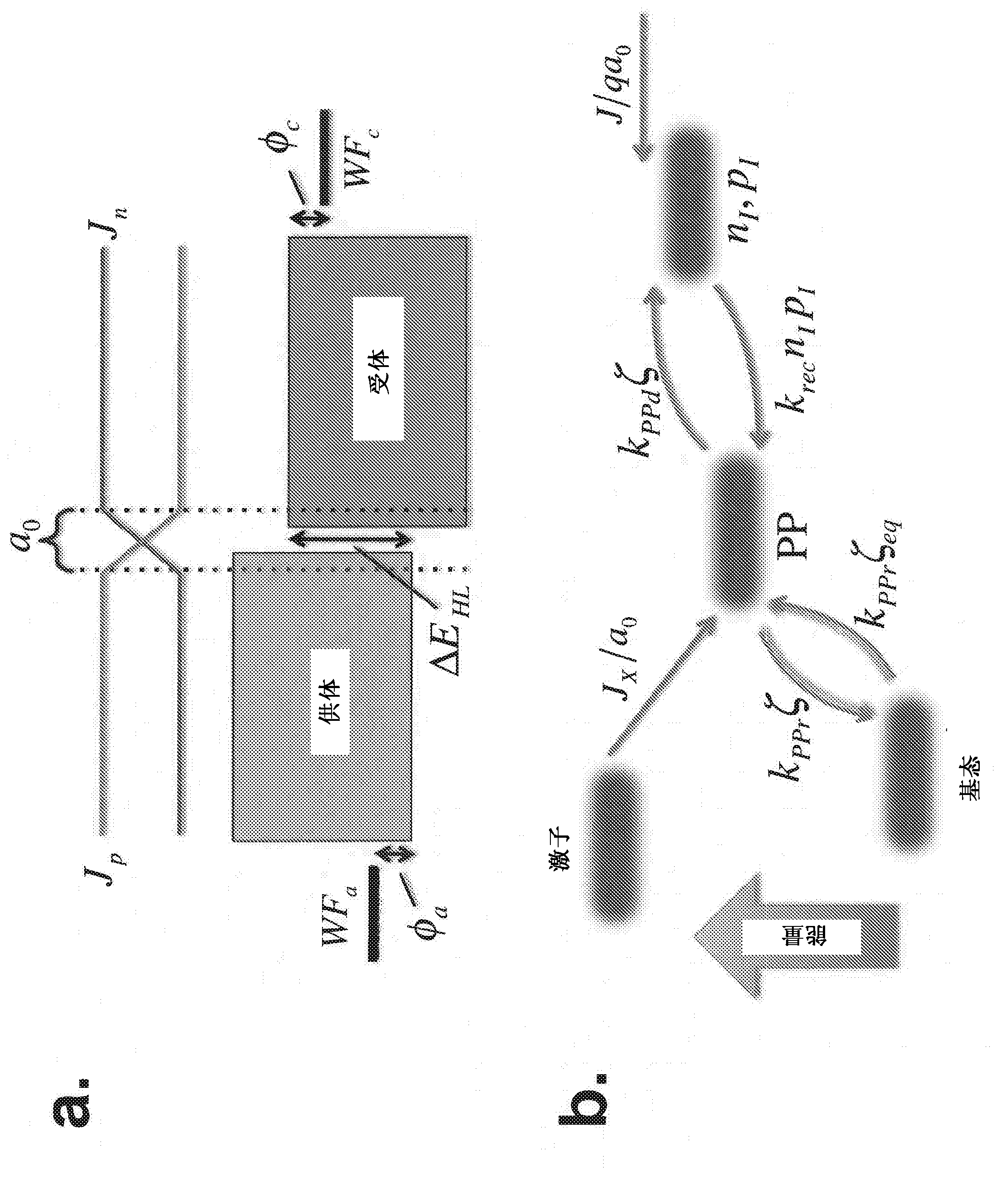
Method of improving exciton dissociation at organic donor-acceptor heterojunctions
A heterojunction and donor technology, which is applied in semiconductor devices, electrical solid state devices, semiconductor/solid state device manufacturing, etc., can solve the problems of non-strict application and lack of physical meaning of parameters, etc.
- Summary
- Abstract
- Description
- Claims
- Application Information
AI Technical Summary
Problems solved by technology
Method used
Image

Examples
Embodiment 1
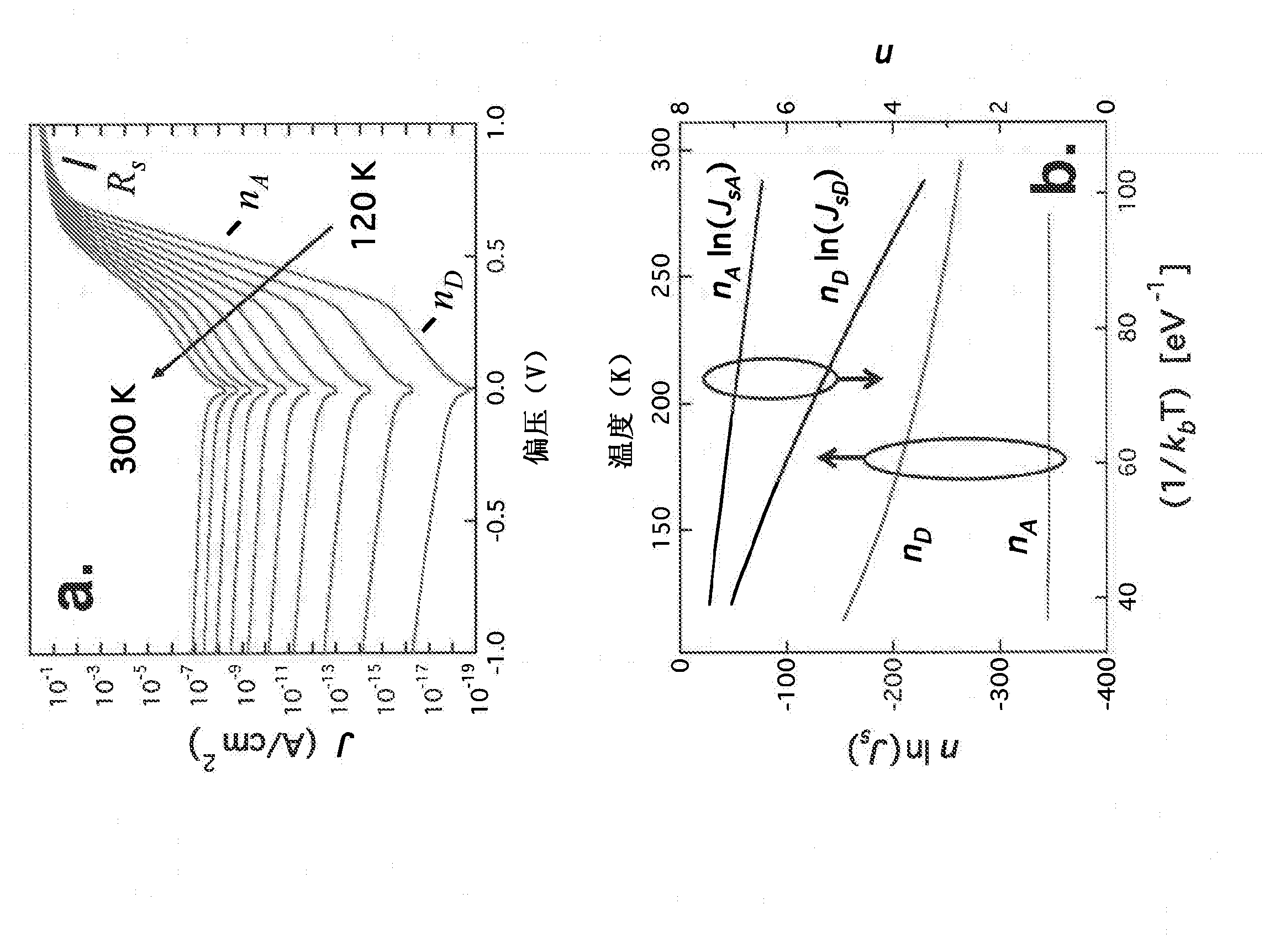
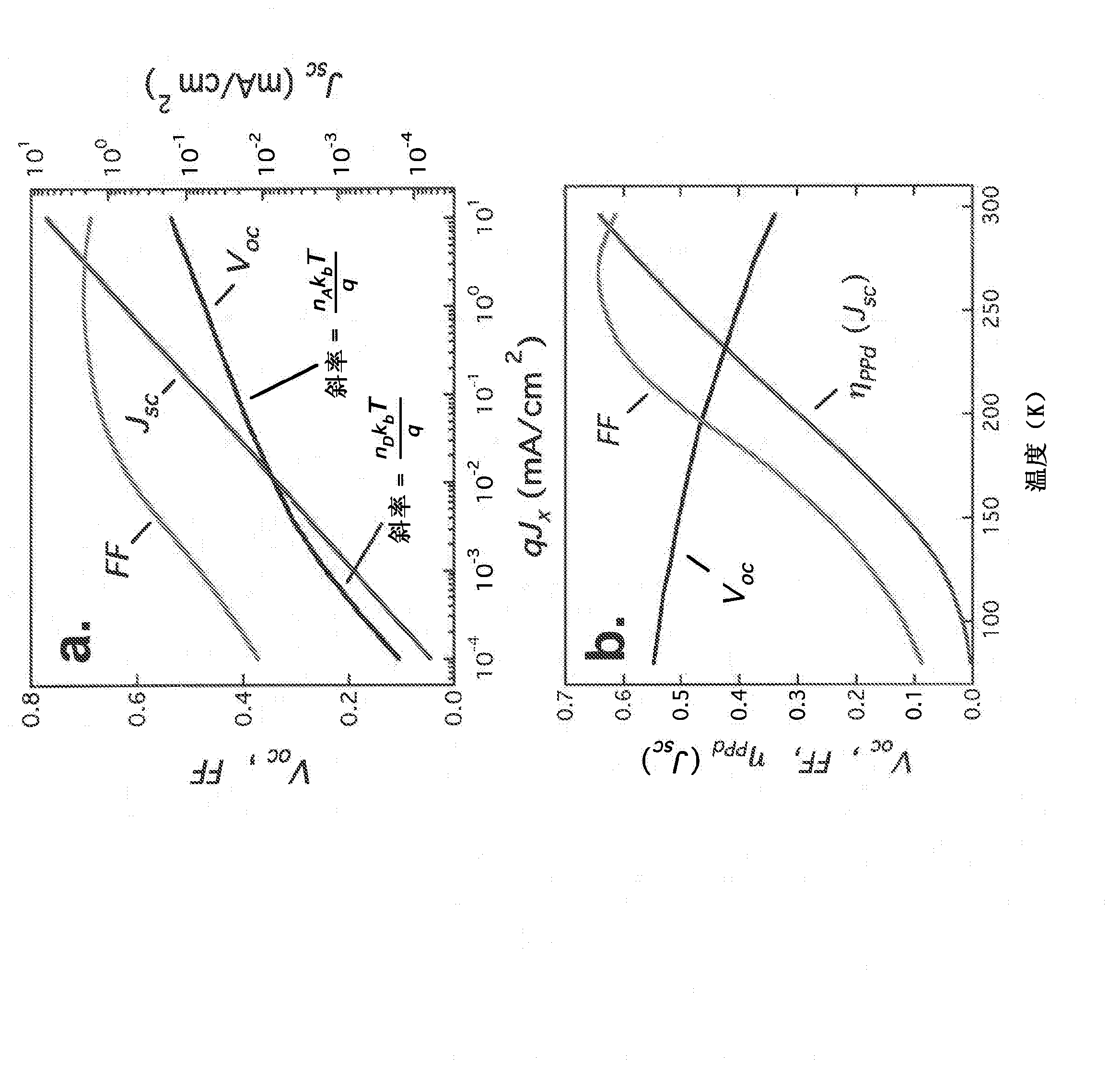
[0206] Fabrication of conventional CuPc / C on glass substrates coated with anodes of transparent indium tin oxide (sheet resistance ~15 ohms / square) pre-patterned into 1 mm wide stripes 60 and SubPc / C 60Battery. All organic materials were purified by thermal gradient sublimation before use. After adequate solvent degreasing of the substrate, at ~10 -7 The sequential deposition of layers was performed by thermal evaporation in a chamber at Torr base pressure. The device is made of 20nm thick CuPc or 11nm thick SubPc followed by 40nm thick C 60 , 10nm-thick bathocuproine and 100nm-thick Al cathode, which are deposited through a mask as 1mm strips placed orthogonally to the patterned anode, forming a 1mm 2 device area.
[0207] The cell efficiency was characterized under simulated AM1.5G irradiation at room temperature in air and found to be comparable to previously reported devices using these material combinations (K.L. Mutolo, E.I. Mayo, B.P. Rand, S.R. Forrest, and M.E. T...
Embodiment 2
[0216] Conventional CuPc / C was fabricated using a method similar to that described in Example 1 60 and SubPc / C 60 battery and conduct property studies. In simple terms, the battery consists of a base pressure of 10 -7 A 20-nm-thick CuPc or 11-nm-thick SubPc layer, followed by a 40-nm-thick C 60 layer, 10nm thick bathocuproine (BCP) and 100nm thick Al cathode.
[0217] Room temperature IMPS is performed in a sealed chamber that can be connected to electricity and light, and the chamber is filled with anhydrous N 2 Purging is continued to minimize device aging. Low temperature data were obtained in a closed-loop, evacuated He cryostat, and the temperature was measured using a Ge thermistor soldered to the surface of the substrate. The use intensity is 30mW / cm 2 Ar + Laser (λ ex =496nm) for excitation; the observed trend is at λ ex =476nm to 514nm range independent of excitation wavelength. A small fraction (2 close to V under IMPS illumination oc τ ~ 5μs is typical fo...
PUM
 Abstract
Description
Claims
Application Information