Method of manufacturing solid-state image pickup element, solid-state image pickup element, image pickup device, electronic apparatus, solid-state image pickup device, and method of manufacturing solid-state image pickup device

A technology of solid-state imaging elements and solid-state imaging devices, which is applied in the direction of electric solid-state devices, radiation control devices, electrical components, etc., can solve problems such as deterioration, sensitivity characteristics and shading characteristics, deviation color reproducibility and sensitivity characteristics, etc., to achieve reduction Loss, the effect of increasing sensitivity

Inactive Publication Date: 2013-04-24
SONY CORP
View PDF16 Cites 10 Cited by
  • Summary
  • Abstract
  • Description
  • Claims
  • Application Information

AI Technical Summary

Problems solved by technology

In this case, when the etching precision is not good, there is a possibility that deviation occurs in the thicknesses of the second-layer color CF and the third-layer color CF and the color reproducibility and sensitivity characteristics are deteriorated accordingly.
In addition, although it is desirable to increase the thickness of CF for the purpose of stopping etching in the middle of the organic film, in this case, there is concern that the light-gathering characteristics of the solid-state imaging device will deteriorate and the sensitivity characteristics and light-shielding characteristics will deteriorate. degraded by it

Method used


Image

  • Method of manufacturing solid-state image pickup element, solid-state image pickup element, image pickup device, electronic apparatus, solid-state image pickup device, and method of manufacturing solid-state image pickup device
  • Method of manufacturing solid-state image pickup element, solid-state image pickup element, image pickup device, electronic apparatus, solid-state image pickup device, and method of manufacturing solid-state image pickup device
  • Method of manufacturing solid-state image pickup element, solid-state image pickup element, image pickup device, electronic apparatus, solid-state image pickup device, and method of manufacturing solid-state image pickup device

Examples


no. 4 example

[0256] 6. Fourth Embodiment (Solid-State Imaging Device and Manufacturing Method Thereof)

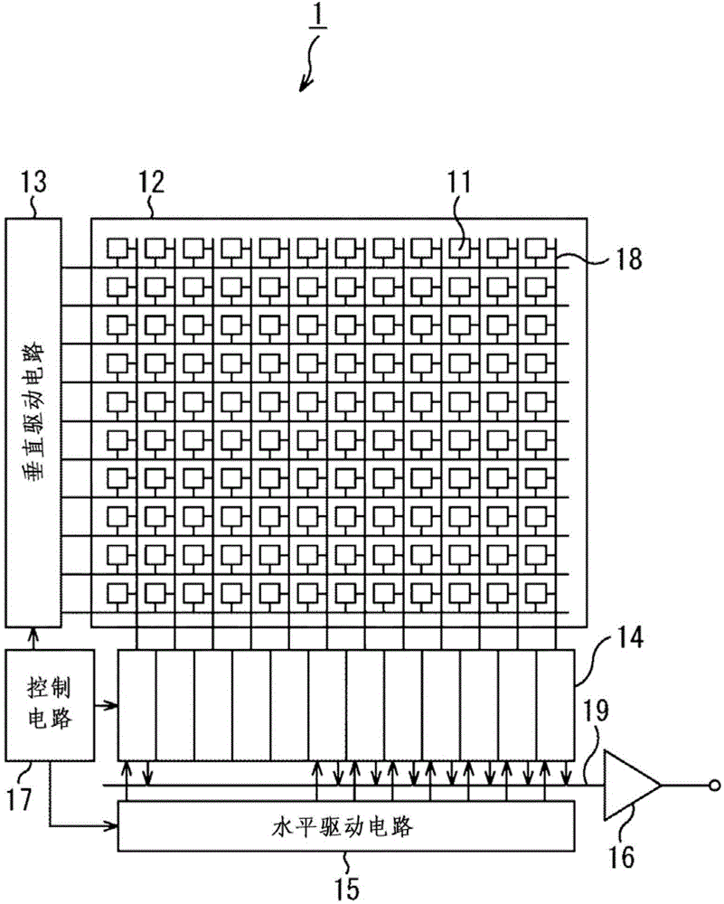
[0257] Figure 9 is a cross-sectional view showing the structure of the main part of the solid-state imaging element of the fourth embodiment of the present invention. Additionally, something like figure 2 The solid-state imaging element 1 of the first embodiment shown in and Figure 4 In the case of the solid-state imaging element 2 of the second embodiment shown in, Figure 9 A cross section of three pixels 11 of the solid-state imaging element 4 of the fourth embodiment is shown. Note that, in the solid-state imaging device 4 of the fourth embodiment, constituent elements corresponding to those in the solid-state imaging device 1 of the first embodiment are denoted by the same reference numerals or symbols, respectively, and are abbreviated here for simplification. Descriptions of them are appropriately omitted.

[0258] The solid-state imaging element 4 of the fourth embodimen...

no. 5 example

[0282] 7. Fifth Embodiment (Solid-State Imaging Device and Manufacturing Method Thereof)

[0283] Cross-sectional view of a pixel

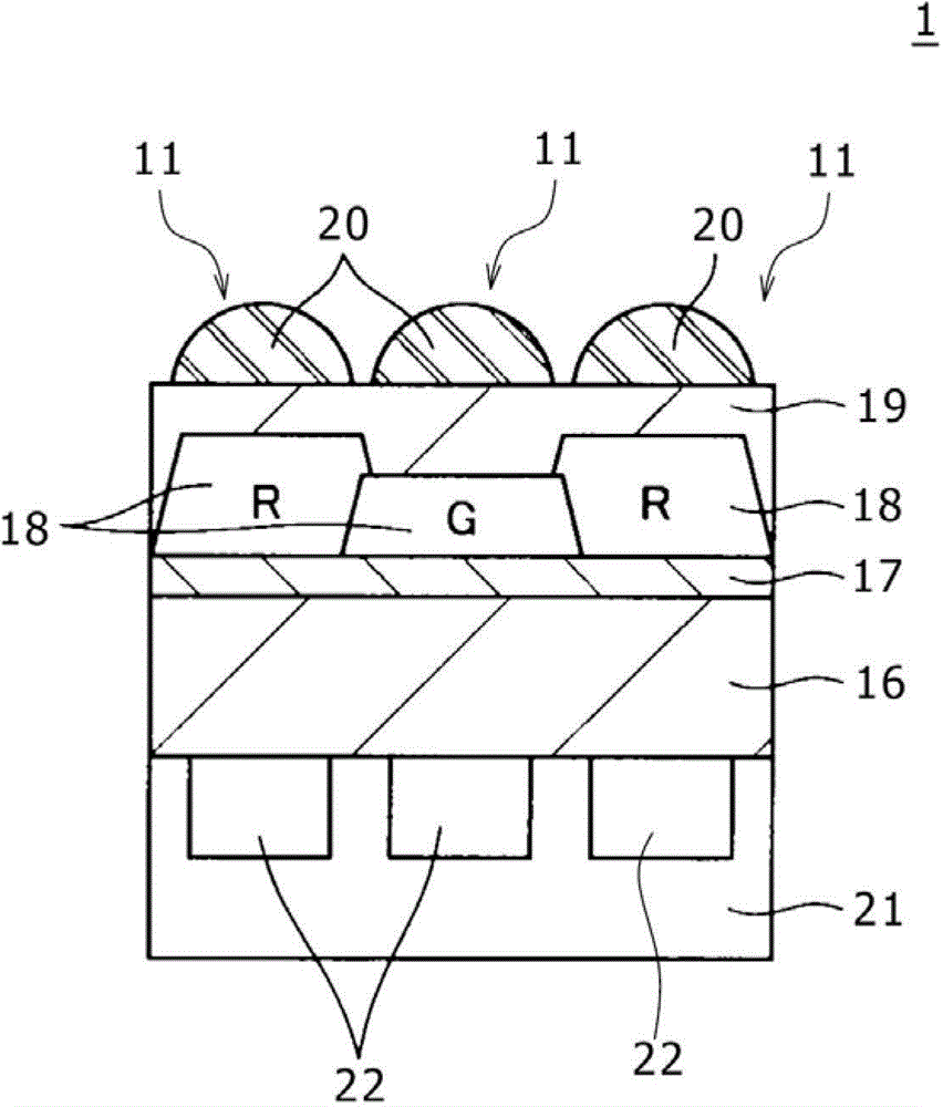
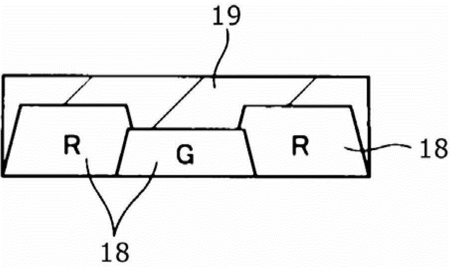
[0284] Figure 18 is a cross-sectional view showing a schematic structure of a pixel 211 within an effective pixel region 2121 of the solid-state imaging element 51 of the fifth embodiment of the present invention.

[0285] In pixel 211, as Figure 18 As shown in , a light receiving region 222 including a photodiode and the like is formed in a semiconductor substrate 221 such as a silicon substrate. A light shielding film 223 is formed in a boundary portion between respective adjacent pixels 211 on the semiconductor substrate 221 , and a planarizing film 224 is formed on the light shielding film 223 . In addition, a red (R), green (G) or blue (B) color filter 225 is formed on the planarization film 224 . As a material of the color filter 225 , a material obtained by adding an R, G, or B pigment as a dye to a photopolymerization negative photos...

no. 6 example

[0316] 8. Sixth Embodiment (Solid-state Imaging Device and Manufacturing Method Thereof)

[0317] Next, the pixel region 212 in the solid-state imaging element 61 of the sixth embodiment of the present invention will be described. It should be noted that, in the solid-state imaging device 61 of the sixth embodiment, constituent elements corresponding to those in the solid-state imaging device 51 of the fifth embodiment are denoted by the same reference numerals or symbols, respectively, and here for Descriptions of them are simplified and appropriately omitted.

[0318] The sixth embodiment is a solid-state imaging element 61 such as Figure 22An embodiment with a cavity structure is shown in . In this case, the effective pixel area 2121 is a concave central portion of the cavity structure, and the invalid pixel area 2122 is a peripheral portion formed slightly higher than the concave central portion. from Figure 22 In the first process shown in , it can be seen that the ...


PUM


Abstract

Disclosed herein are a method of manufacturing solid-state image pickup elements, a solid-state image pickup element, an image pickup device, an electronic apparatus, a solid-state image pickup device, and a method of manufacturing the solid-state image pickup device. The solid-state image pickup element has a lens provided above a light receiving portion. The manufacturing method includes: forming a lens base material layer composing the lens; forming an intermediate film having a thermal expansion coefficient larger than that of a resist on the lens base material layer; forming the resist in contact with the intermediate film; forming the resist into a lens shape by thermal reflow; and transferring the lens shape of the resist to the lens base material layer by etching, thereby forming the lens. The solid-state image pickup element reduces lens invalid areas and the methods maintain machining precision, and characteristic degradation of the solid-state image pickup element is restrained and the solid-state image pickup elements are easier to manufacture.

Description

[0001] Cross References to Related Applications [0002] This application contains references to Japanese Priority Patent Applications JP 2011-231640, JP 2011-262101 and JP 2011-268895 filed with the Japan Patent Office on October 21, 2011, November 30, 2011 and December 8, 2011, respectively The subject matter to which the disclosure is based, these priority applications are hereby incorporated by reference in their entirety. technical field [0003] The present invention relates to a method for manufacturing a solid-state imaging device, a solid-state imaging device manufactured by the manufacturing method, an imaging device including the solid-state imaging device, electronic equipment including the imaging device, a solid-state imaging device, and a manufacturing method thereof. Background technique [0004] In a solid-state imaging device, a microlens is provided above the light-receiving portion of each pixel in order to increase the light-collecting efficiency and the...

Claims


Application Information

Patent Timeline
Patent Type & Authority Applications(China)
IPC IPC(8): H01L27/146
CPCH01L27/14685H01L27/14627H01L27/14621H01L27/146
Inventor 荻野明子山本笃志大塚洋一东宫祥哲
Owner SONY CORP
Why Eureka
Try Eureka