Organic light emitting diode (OLED) device

A device and structural technology, applied in the field of organic electroluminescence devices, can solve the problems that OLED devices cannot satisfy the requirements of good brightness and long life at the same time, and achieve the effects of wide application range, good service life and improved device life.

Active Publication Date: 2013-04-24
KUNSHAN VISIONOX DISPLAY TECH +2
View PDF6 Cites 4 Cited by
  • Summary
  • Abstract
  • Description
  • Claims
  • Application Information

AI Technical Summary

Problems solved by technology

[0009] For this reason, the technical problem to be solved by the present invention lies in the problems in the prior art that OLED devices cannot meet the requirements of good brightness and long service life at the same time due to defects in luminescent materials, and then provide a new luminescent material that can meet the requirements for brightness at the same time. and OLED devices with lifetime requirements

Method used


Image

  • Organic light emitting diode (OLED) device
  • Organic light emitting diode (OLED) device
  • Organic light emitting diode (OLED) device

Examples


Embodiment 1

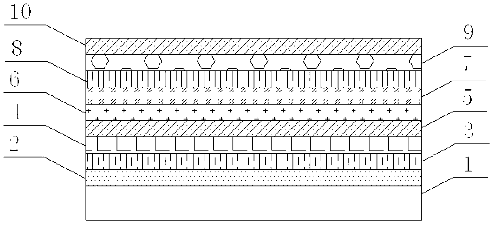
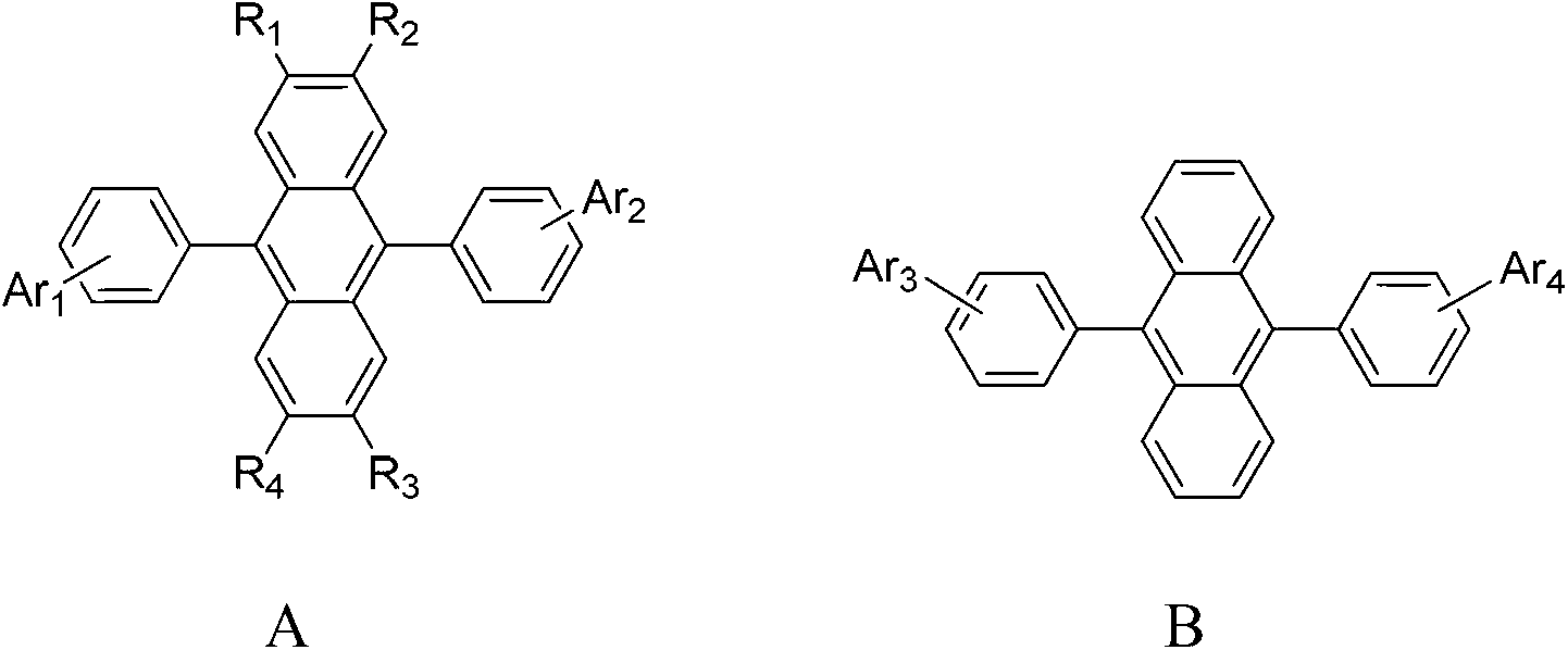
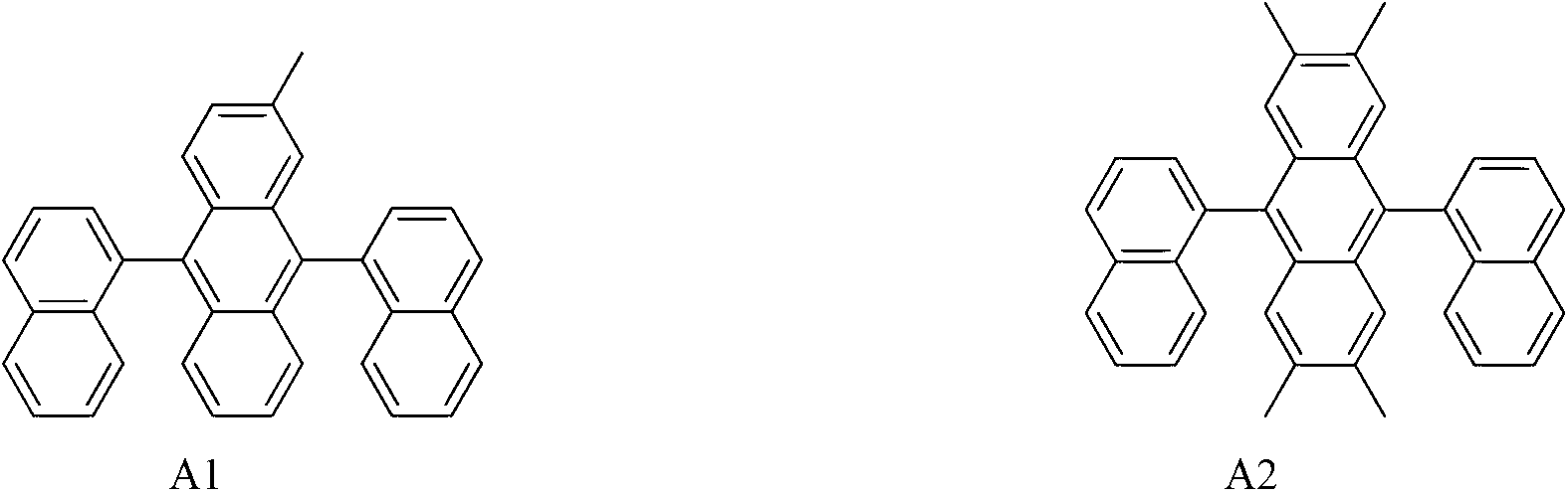
[0057] Red light devices: such as figure 1 As shown, the substrate 1 is a glass substrate. On the substrate 1, Ag is sputtered and deposited as the reflective layer 2 with a thickness of 150nm. ITO of 10nm is sputtered as the anode 3 of the device, and the required pattern is etched out. 3 Plasma treatment for 3 minutes. The resulting substrate 1 was placed in a vacuum, and 130 nm of MTDATA was deposited as a hole injection layer (HIL) 4 by co-evaporation. Next, 10 nm of NPB was deposited as a hole transport layer (HTL) 5 . Then take the compound shown in A1 and the compound shown in B1 according to the mass ratio of 1:1 and mix to obtain the required host material, and add the guest material Ir(piq) which accounts for 5% of the host material by mass 2 (acac), using a double-source co-evaporation method, preheating the two in the evaporation source under a vacuum environment, and vapor-depositing them on the substrate to prepare the light-emitting layer with a thickness of 3...

Embodiment 2

[0063] The structure and specific implementation steps of the OLED device described in this example are the same as those of the red light device in Example 1, the only difference being that the host material is composed of the compound shown in formula A2 and the compound shown in formula B3 in a mass ratio of 5:10 mix.

Embodiment 3

[0065] The structure and specific implementation steps of the OLED device described in this example are the same as those of the red light device in Example 1, the only difference being that the host material is composed of the compound shown in formula A3 and the compound shown in formula B4 in a mass ratio of 6:10 mix.


PUM

PropertyMeasurementUnit
thicknessaaaaaaaaaa
thicknessaaaaaaaaaa
thicknessaaaaaaaaaa

Abstract

The invention belongs to the field of organic electroluminescence devices, and particularly relates to an organic light emitting diode (OLED) device utilizing organic electroluminescence material as a lighting layer. According to the OLED, the lighting material forming the lighting layer comprises subject material and object material, wherein the subject material comprises compound shown in a structural formula A, and compound shown by a structural formula B in a mixed mode, and the weight proportion of the compound shown in the structural formula A, and the compound shown by the structural formula B is 1-20:10. According to the OLED device, the compound shown by the structural formula A, high in steric hindrance, and the compound shown by the structural formula B, high in electronic mobility, are utilized for the organic electroluminescence material utilizes the compound, the proportion relation of the two compounds is adjusted and optimized to adjust electronic transmission performance of a new subject, and therefore a device having good luminance and long service life is obtained.

Description

technical field [0001] The invention belongs to the field of organic electroluminescent devices, and in particular relates to an organic electroluminescent material and its application in light emitting devices. Background technique [0002] The phenomenon of electroluminescence was first discovered in the 1930s. The original luminescent material was ZnS powder, from which LED technology was developed, and now it is widely used in energy-saving light sources. The phenomenon of organic electroluminescence was first discovered by Pope et al. in 1963. They found that the single-layer crystal of anthracene can emit weak blue light under the drive of voltage above 100V. Until 1987, Dr. Deng Qingyun of Kodak Company made organic fluorescent dyes into double-layer devices by vacuum evaporation. When the driving voltage was less than 10 volts, the external quantum efficiency reached 1%, making organic electroluminescent materials And devices have the possibility of practicability, ...

Claims


Application Information

Patent Timeline
Patent Type & Authority Applications(China)
IPC IPC(8): H01L51/52H01L51/54C09K11/06
Inventor 邱勇刘宏俊
Owner KUNSHAN VISIONOX DISPLAY TECH
Why Eureka
Try Eureka