Multi-junction solar battery and preparation method thereof

A technology of solar cells and manufacturing methods, applied in circuits, photovoltaic power generation, electrical components, etc., can solve problems such as lattice mismatch, achieve the effect of reducing dislocation density and broadening the spectral absorption range

Inactive Publication Date: 2013-05-01
TIANJIN SANAN OPTOELECTRONICS
View PDF1 Cites 3 Cited by
  • Summary
  • Abstract
  • Description
  • Claims
  • Application Information

AI Technical Summary

Problems solved by technology

In 0.3 Ga 0.7 As has a band gap of 1eV and is one of the best c

Method used


Image

  • Multi-junction solar battery and preparation method thereof
  • Multi-junction solar battery and preparation method thereof
  • Multi-junction solar battery and preparation method thereof

Examples


Embodiment 1

[0055] This embodiment discloses a flip-chip five-junction solar cell, and its structure will be specifically described below in conjunction with a growth method.

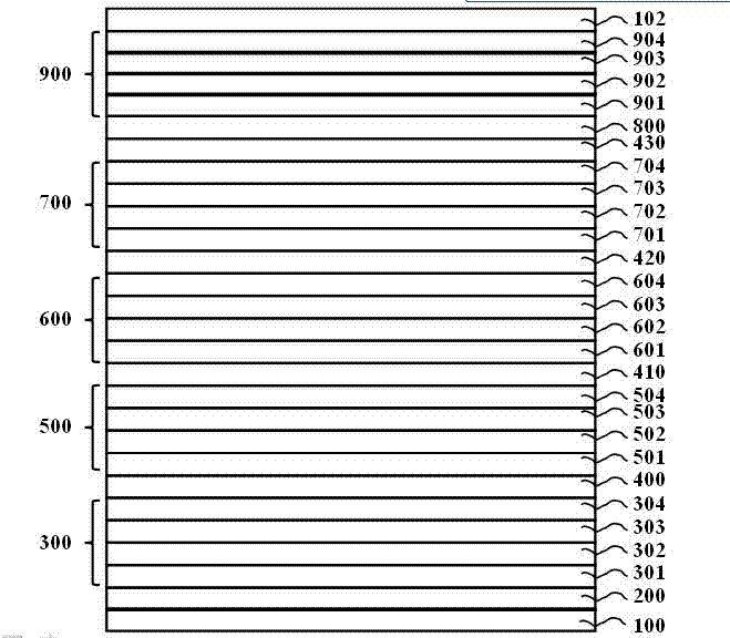
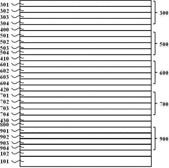
[0056] First, in the MOCVD system, a p-type GaAs substrate 100 is selected, and its doping concentration is 2×10 17 cm -3 -- 5×10 17 cm -3 ; Epitaxial growth of GaInP on the surface of the substrate etch the cut-off layer 200, its thickness is 150 nm, and the doping is about 1×10 18 cm -3 .

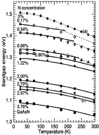
[0057]In the next step, the AlGaInP first sub-cell 300 is flip-chip grown on the etching cut-off layer 200, and its band gap is 2.2 eV, specifically including: n-type AlGaInP window layer 301, its thickness is 25 nm, and the doping concentration is 1×10 18 cm -3 around; the thickness of the emitting region 302 is 150 nm, and the doping concentration is 2×10 18 cm -3 ; The preferred thickness of the base region 303 is 900 nm, and the doping concentration is 5×10 17 cm -3 ; The p-type AlGaInP back field layer 304 has ...

Embodiment 2

[0071] This embodiment discloses a flip-chip four-junction solar cell. On the basis of Implementation 1, the first AlGaInP sub-cell 300 can be removed, and the second GaInP sub-cell 500 can be used as the first sub-cell of this embodiment to form a 1.89 eV / 1.65 eV / 1.4 eV / 1 eV flip-chip four-junction solar cells.

Embodiment 3

[0073] This embodiment discloses a flip-chip four-junction solar cell, and the GaInP second sub-cell 500 can be removed on the basis of implementation one to form a 2.2 eV / 1.65 eV / 1.4 eV / 1 eV flip-chip four-junction solar cell.


PUM

PropertyMeasurementUnit
Bandgapaaaaaaaaaa
Bandgapaaaaaaaaaa
Bandgapaaaaaaaaaa

Abstract

The invention discloses a reverse multi-junction solar battery and a preparation method thereof. The multi-junction solar cell comprises a substrate, a first sub-battery, a second sub-battery, a third sub-battery, a fourth sub-battery, a gradient buffering layer and a fifth sub-battery, wherein the first sub-battery reversely grows on the substrate and is provided with a first band gap; the second sub-battery is reversely formed on the first sub-battery and is provided with a second band gap smaller than the first band gap; the third sub-battery is reversely formed on the second sub-battery and is provided with a third band gap smaller than the second band gap; the fourth sub-battery is reversely formed on the third sub-battery and is provided with a fourth band gap smaller than the third band gap; the first sub-battery, the second sub-battery, the third sub-battery and the fourth sub-battery are in lattice matching with the substrate; the gradient buffering layer is formed on the fourth sub-battery, is used for overcoming the lattice mismatching between the fourth sub-battery and the fifth sub-battery and is provided with a fifth band gap smaller than the fourth band gap; and the fifth sub-battery is reversely formed on the homogeneous gradient buffering layer and is provided with a sixth band gap smaller than the fifth band gap. Through various later-stage processes, the required solar battery is obtained. The high-efficiency multi-junction solar battery with current matching and wider spectral-absorbing range can be prepared through the invention.

Description

technical field [0001] The invention relates to a multi-junction solar cell and a preparation method thereof, belonging to the technical field of semiconductor materials. Background technique [0002] In recent years, solar cells have attracted more and more attention as a practical new energy source. It is a semiconductor device that uses the photovoltaic effect to convert solar energy into electrical energy, which greatly reduces people's dependence on coal, oil and natural gas in production and life, and has become one of the most effective ways to use green energy. Among all new energy sources, solar energy is one of the most ideal renewable energy sources, and fully developing and utilizing solar energy has become an energy strategic decision for sustainable development of governments around the world. In recent years, as the third-generation photovoltaic power generation technology, concentrating multi-junction compound solar cells have attracted much attention becaus...

Claims


Application Information

Patent Timeline
IPC IPC(8): H01L31/0352H01L31/078H01L31/18
CPCH01L31/076H01L31/078H01L31/18H01L31/0687H01L31/0725Y02E10/50H01L31/03048Y02E10/544Y02E10/548Y02P70/50
Inventor 毕京锋林志东蔡文必林桂江刘建庆宋明辉丁杰
Owner TIANJIN SANAN OPTOELECTRONICS
Why Eureka
Try Eureka