Silver-bismuth superlattice nanowire array and preparation method and application thereof

A technology of nanowire arrays and silver nanowires, which is applied in nanotechnology, nanotechnology, and the preparation of test samples, can solve problems such as difficult to obtain accurate and controllable sizes, achieve melting test signal enhancement, scientific preparation methods, and eliminate The effect of mutual influence

Inactive Publication Date: 2013-05-08
HEFEI INSTITUTES OF PHYSICAL SCIENCE - CHINESE ACAD OF SCI
View PDF7 Cites 10 Cited by
  • Summary
  • Abstract
  • Description
  • Claims
  • Application Information

AI Technical Summary

Problems solved by technology

For the melting of nanomaterials, at present, people have theoretically studied the size-dependent melting characteristics of nanoparticles and nanowires, and experimental research on the melting of metal nanomaterials mostly focuses on nanoparticles. The main reason is that it is difficult to obtain metal nano-samples with precise and controllable sizes and which can be used for melting tests

Method used


Image

  • Silver-bismuth superlattice nanowire array and preparation method and application thereof
  • Silver-bismuth superlattice nanowire array and preparation method and application thereof

Examples


Embodiment 1

[0031] The concrete steps of preparation are:

[0032] Step 1, first use the secondary anodic oxidation method to obtain a through-hole alumina template with a hole diameter of 55nm, and then plate a gold film on one side of the through-hole alumina template.

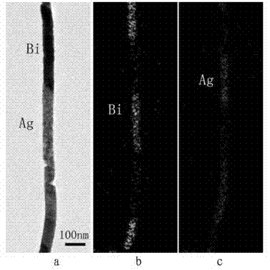
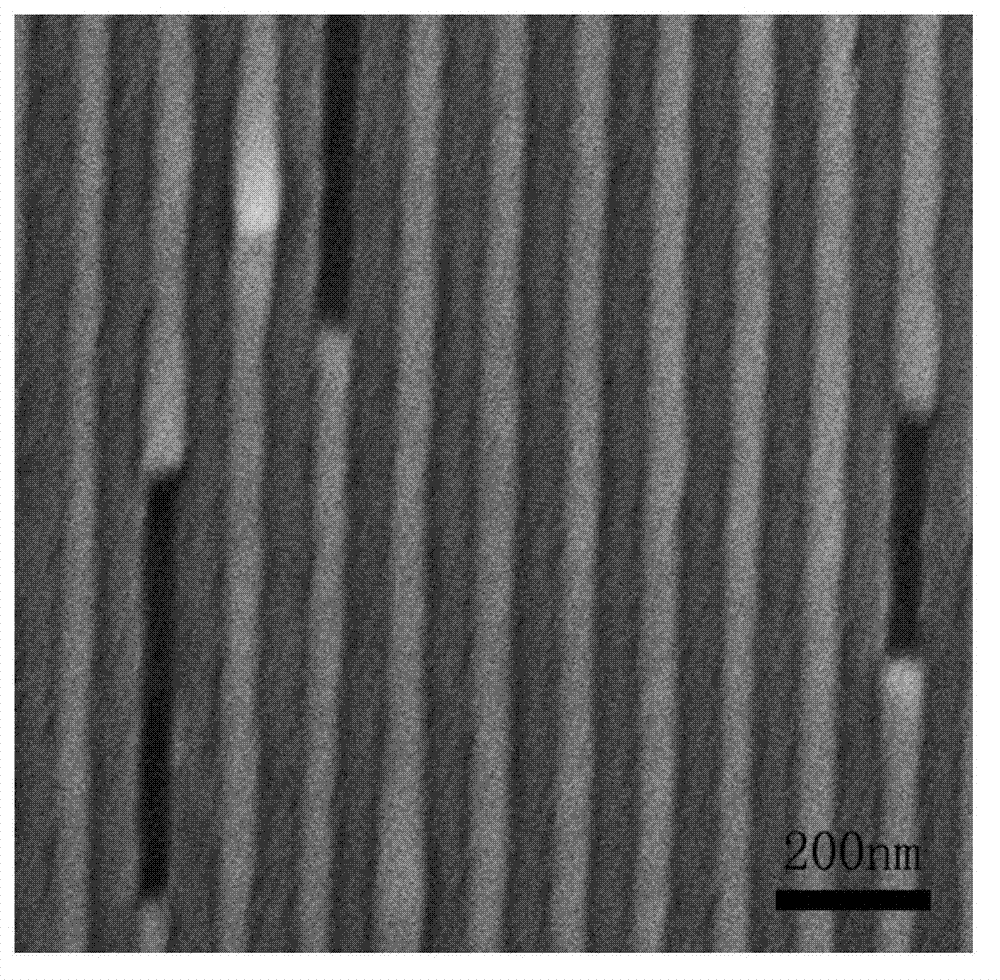
[0033] Step 2, first place the aluminum oxide template coated with a gold film on one side in the silver electrolyte, and after electrodeposition at a DC voltage of 0.4V for 35 seconds, soak and clean it in deionized water for 1 minute. Then it was placed in a bismuth electrolyte, and after being electrodeposited at a DC voltage of 0.9V for 600s, it was soaked and cleaned in deionized water for 1 min. Repeat the above steps to place the aluminum oxide templates coated with a gold film on one side in the silver electrolyte and bismuth electrolyte in turn for electrodeposition, and the number of cycles of immersion and cleaning in deionized water is 2 times, and the approximate figure 1 and figure 2 The silver-bismuth ...

Embodiment 2

[0035] The concrete steps of preparation are:

[0036] Step 1, first use the secondary anodic oxidation method to obtain a through-hole alumina template with a hole diameter of 58nm, and then plate a gold film on one side of the through-hole alumina template.

[0037] Step 2, first place the aluminum oxide template coated with a gold film on one side in the silver electrolyte, electrodeposit it at a DC voltage of 0.45V for 33s, then soak and clean it in deionized water for 2min. Then it was placed in a bismuth electrolyte, and after being electrodeposited at a DC voltage of 1.0 V for 460 s, it was soaked in deionized water and cleaned for 2 min. Repeat the above steps to place the aluminum oxide template coated with a gold film on one side in the silver electrolyte and bismuth electrolyte in turn for electrodeposition, and the number of cycles of immersion and cleaning in deionized water is 4 times. figure 1 and figure 2 The silver-bismuth superlattice nanowire array shown....

Embodiment 3

[0039] The concrete steps of preparation are:

[0040] Step 1, first use the secondary anodic oxidation method to obtain a through-hole alumina template with a hole diameter of 60nm, and then plate a gold film on one side of the through-hole alumina template.

[0041] Step 2, first place the aluminum oxide template coated with a gold film on one side in a silver electrolyte, and after electrodeposition at a DC voltage of 0.5V for 30 seconds, soak and clean it in deionized water for 3 minutes. Then it was placed in a bismuth electrolyte, and after being electrodeposited at a DC voltage of 1.1V for 320s, it was soaked and cleaned in deionized water for 3 minutes. Repeat the above steps to place the aluminum oxide templates coated with a gold film on one side in the silver electrolyte and bismuth electrolyte for electrodeposition, and place the number of cycles of immersion and cleaning in deionized water for 6 times to obtain the following: figure 1 and figure 2 The silver-bi...


PUM

PropertyMeasurementUnit
thicknessaaaaaaaaaa
lengthaaaaaaaaaa
lengthaaaaaaaaaa

Abstract

The invention discloses a silver-bismuth superlattice nanowire array and a preparation method and application thereof. The array is formed by arranging one-dimensional superlattice nanowires which are formed by alternately connecting silver nanowires and bismuth nanowires in holes of an alumina template with a gold film coated on one surface, wherein the thickness of the gold film is 200-400nm, the linear diameter of the silver nanowires is 55-65nm, the silver nanowires are 100-200nm long, the linear diameter of the bismuth nanowires is 55-65nm, and the bismuth nanowires are 65nm-2mum long. The method comprises the following steps of firstly obtaining a through hole alumina template with a hole diameter of 55-65nm through a two-step anodic oxidation method, then plating the gold film on one surface of the through hole alumina template, next, placing the alumina template with one side plated with the gold film in silver electrolyte, electro-depositing for 25-35s at direct-current voltage of 0.4-0.6V, then placing the alumina template in bismuth electrolyte, and electro-depositing for 45-600s at direct-current voltage of 0.9-1.3V so as to prepare the silver-bismuth superlattice nanowire array. The silver-bismuth superlattice nanowire array can be used for testing the relationship between the length-diameter ratio and the melting characteristic of the bismuth nanowire.

Description

technical field [0001] The invention relates to a nanowire array, its preparation method and application, in particular to a silver-bismuth superlattice nanowire array, its preparation method and application. Background technique [0002] In 1970, Jiang Qi and Zhu Zhaoxiang of the IBM laboratory in the United States proposed the concept of superlattice, that is, artificially make the structure of the prepared material change periodically, when the modulation period is several times or longer than the lattice constant of the material , is called a superlattice. Extending the definition of superlattice to the structure of one-dimensional nanomaterials results in the emergence of one-dimensional superlattice nanowires, which usually refer to one-dimensional periodic nanostructures formed by the periodic arrangement of two materials. For the melting of nanomaterials, at present, people have theoretically studied the size-dependent melting characteristics of nanoparticles and na...

Claims


Application Information

Patent Timeline
Patent Type & Authority Applications(China)
IPC IPC(8): C25D11/12C25D11/18C25D11/16C25D5/10C25D3/46C25D3/54G01N1/28B82Y30/00B82Y40/00
Inventor 游巧费广涛许少辉
Owner HEFEI INSTITUTES OF PHYSICAL SCIENCE - CHINESE ACAD OF SCI
Why Eureka
Try Eureka