

Gallium nitride (GaN) base light-emitting diode (LED) structure and method for improving photoelectric conversion efficiency thereof
An LED structure, p-electrode technology, applied in circuits, electrical components, semiconductor devices, etc., can solve problems such as low photoelectric conversion efficiency, and achieve the effects of improving photoelectric conversion efficiency, reducing reverse current, and reducing reverse current.
- Summary
- Abstract
- Description
- Claims
- Application Information
AI Technical Summary
Problems solved by technology
Method used
Image

Examples
Embodiment Construction
[0026] The principles and features of the present invention are described below in conjunction with the accompanying drawings, and the examples given are only used to explain the present invention, and are not intended to limit the scope of the present invention.
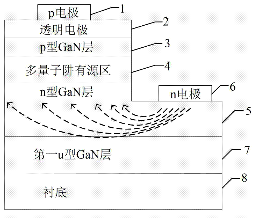
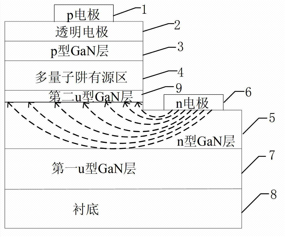
[0027] like figure 2 As shown, this embodiment provides a GaN-based LED structure, which includes a p-electrode 1, a transparent electrode 2, a p-type GaN layer 3, a multi-quantum well active region 4, an n-type GaN layer 5, n-electrode 6, first u-type GaN layer 7 and substrate 8, and a second u-type GaN layer 9 is inserted in the multi-quantum well active region 4 and the n-type GaN layer 5.
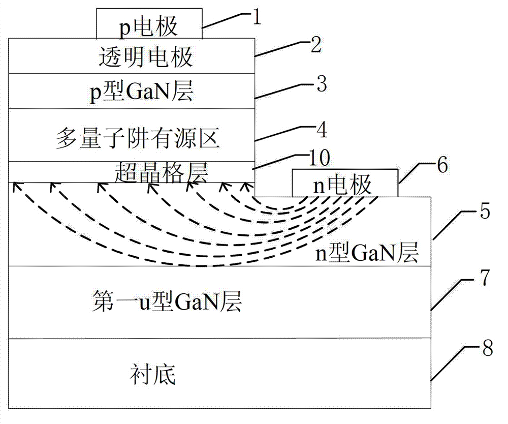
[0028] like image 3 As shown, there is another improvement in this embodiment, that is, a superlattice layer 10 is inserted in the multi-quantum well active region 4 and the n-type GaN layer 5, and the superlattice layer 10 is made of u-Al x Ga 1-x A superlattice layer 10 formed by alternate growth of N layers and low-d...
PUM
 Abstract
Description
Claims
Application Information