Semiconductor laser emitting from vertical and extended cavity surface used for electric pump
A laser, electric pumping technology, applied in semiconductor lasers, lasers, laser parts and other directions, can solve the problems of non-compliance, high technical difficulty, damage to the active area of the device, etc., to achieve improved efficiency, high output power, low series connection The effect of resistance
- Summary
- Abstract
- Description
- Claims
- Application Information
AI Technical Summary
Problems solved by technology
Method used
Image
Examples
Embodiment 1
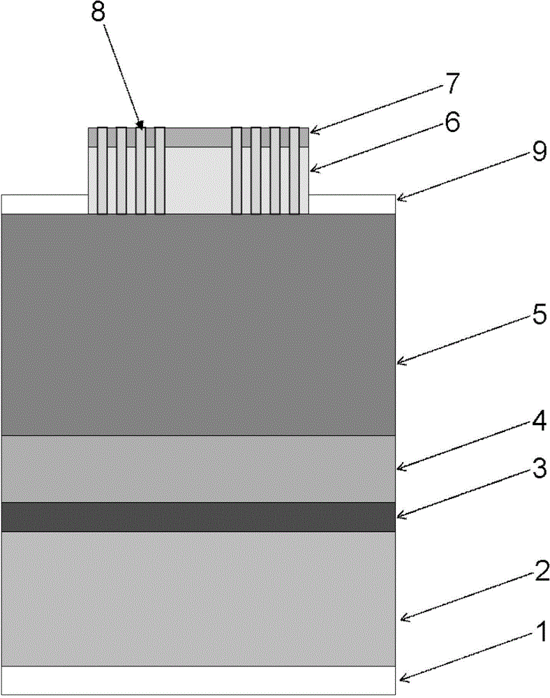
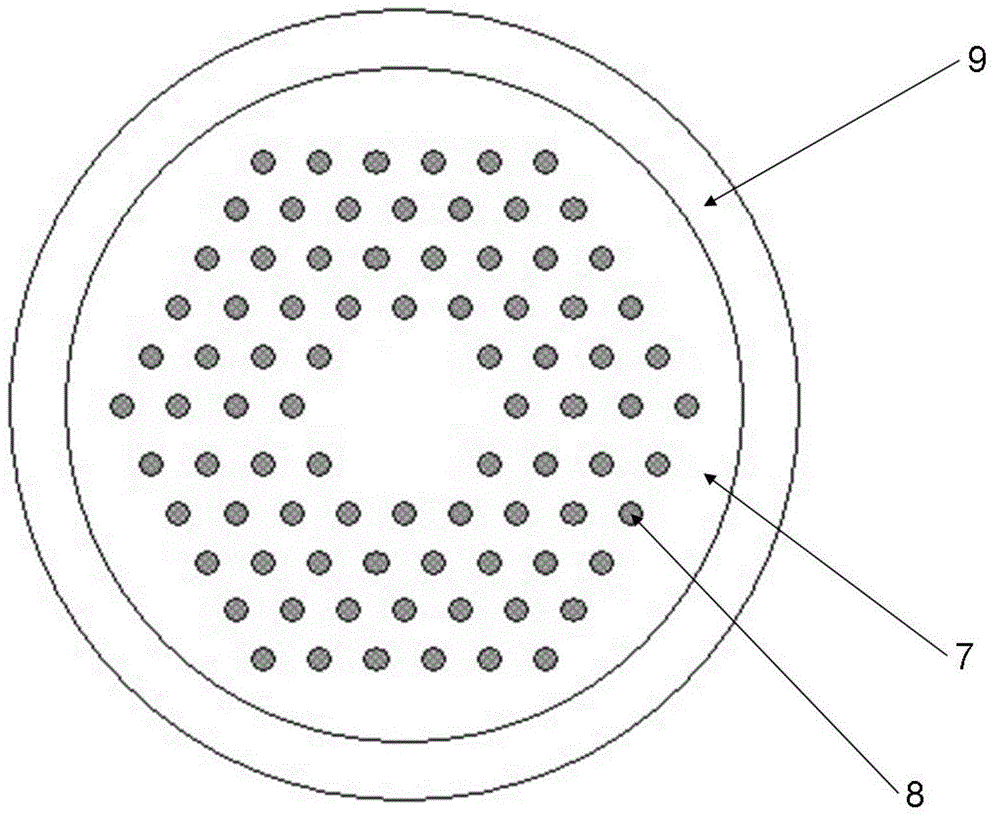
[0033]For the output light with a lasing wavelength of 980nm, the active layer 3 is a continuous laser power supply, the P-type DBR layer 2 is 20 pairs of AlGaAs / GaAs, the first N-type DBR layer 4 is 10 pairs of AlGaAs / GaAs, and the substrate layer 5 is GaAs , the second N-type DBR layer 6 is 20 pairs of AlGaAs / GaAs, the epitaxial anti-reflection layer 7 is a group of AlAs thin films with stepwise changes in Al composition, and a dry method is used on the epitaxial anti-reflection layer 7 and the second N-type DBR layer 6 The photonic crystal defect microcavity structure 8 with a periodic structure is produced by etching technology, the active layer 3 is a periodic InGaAs / GaAsP multi-quantum well structure, including InGaAs quantum wells and GaAsP barriers, and the lower electrode 1 is 10 pairs of Ti / The Au metal thin film, the upper electrode 9 is an AuGeNi / Au thin film, so that a 980nm electrically pumped vertically extended cavity surface-emitting semiconductor laser can be...
Embodiment 2
[0035] The material of the P-type DBR layer 2 in Example 1 is changed to InP / InGaAsP, and the logarithm is changed to 40 pairs. The material of the first N-type DBR layer 4 is changed to InP / InGaAsP, and the logarithm is changed to 20 pairs. The second N-type The material of DBR layer 6 is changed to InP / InGaAsP, the logarithm is changed to 40 pairs, the active layer 3 is changed to a periodic InGaAsP / InP multi-quantum well structure, the material of substrate layer 5 is changed to InP material, the bottom electrode 1, and the epitaxial anti-reflection layer 7. The photonic crystal defect microcavity structure 8 with periodic structure and the upper electrode 9 remain unchanged, so that a 1550nm electrically pumped vertically extended cavity surface-emitting semiconductor laser can be obtained, and a high-power single transverse mode laser output in the 1550nm band can be obtained.
PUM
 Abstract
Description
Claims
Application Information

