
Manufacturing method for structure of wafer level light emitting diode matrix

A technology of light-emitting diodes and array structures, which is applied to electrical components, electrical solid-state devices, circuits, etc., can solve the problems of cumbersome and complicated processes, high yield requirements, and longer production cycles, and achieve simple operation, high yield, and The effect of simplifying the production process

Active Publication Date: 2013-05-15
INST OF SEMICONDUCTORS - CHINESE ACAD OF SCI
View PDF4 Cites 32 Cited by
  • Summary
  • Abstract
  • Description
  • Claims
  • Application Information

AI Technical Summary

Problems solved by technology

[0005] As mentioned before, the preparation of LED flat-panel displays by using surface-mounted LEDs only needs to fix the pre-packaged surface-mounted LEDs on the substrate, while the production process using chip flip-chip technology requires different light colors The light-emitting diodes are welded on the substrate one by one in order to form a plurality of light-emitting diode units, and then the light-emitting diode array formed by a large number of light-emitting diode units is used as a display panel. Therefore, the display array is prepared by flip-chip technology, especially When it is a large-area display array, the entire process is cumbersome and complicated, the production cycle becomes longer, and the yield rate is too high

Method used


Image

  • Manufacturing method for structure of wafer level light emitting diode matrix
  • Manufacturing method for structure of wafer level light emitting diode matrix
  • Manufacturing method for structure of wafer level light emitting diode matrix

Examples


Embodiment Construction

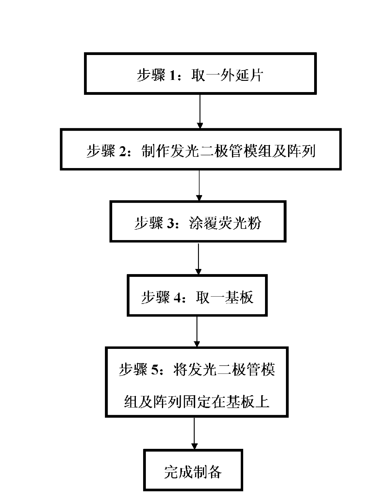
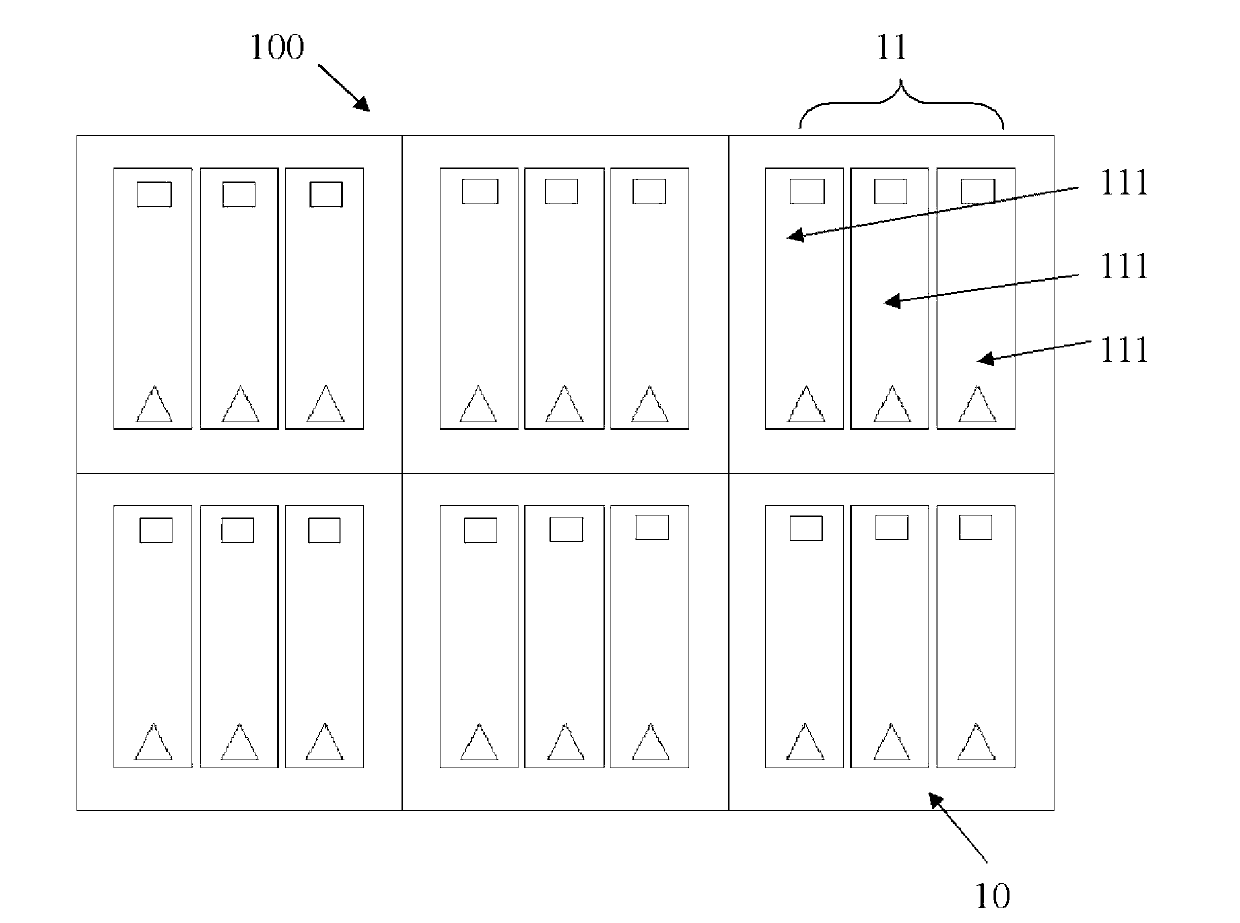
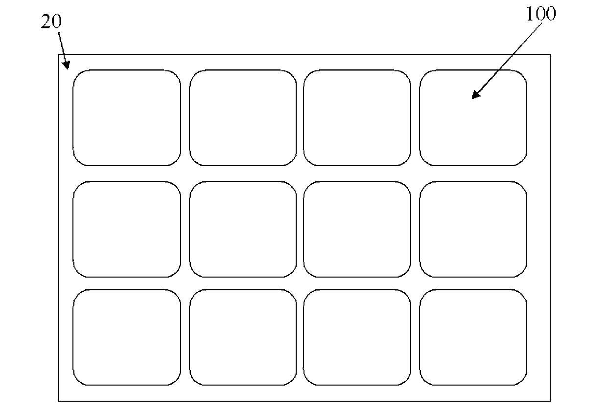
[0018] see Figure 1 to Figure 3 As shown, the present invention provides a method for preparing a wafer-level light-emitting diode array structure, comprising the following steps:

[0019] Step 1: Take an epitaxial wafer 10, and the material of the epitaxial wafer can be III-V group semiconductor material, such as GaAs, GaN and so on. Epitaxial materials can be obtained by vapor phase epitaxy or metal organic compound chemical vapor deposition techniques. Taking GaN materials as an example, epitaxial materials can be grown on sapphire, silicon carbide or silicon substrates, and the growth of epitaxial wafers can also be completed on GaN self-supporting substrates. The epitaxial wafer includes an n-type layer, an active layer and a p-type layer.

[0020] Step 2: Prepare light-emitting diode unit module 11 on epitaxial wafer 10 (see figure 2 ), forming an LED array 100, the LED unit module 11 includes a plurality of LEDs 111; the number of each group of LEDs 111 in the LED ...


PUM


Abstract

Disclosed is a manufacturing method for a structure of a wafer level light emitting diode matrix. The method includes the following steps: step1, wherein an epitaxial wafer is taken; step2, wherein a light emitting diode unit module is manufactured on the epitaxial wafer to form a light emitting diode matrix, and the light emitting diode unit module comprises a plurality of light emitting diodes; step3, wherein fluorescent powder is coated on the light emitting diodes in the light emitting diode unit module, the light emitting diodes motivates the fluorescent powder to produce light with different wavelengths, so that output light and color of the light emitting diodes are adjusted; step4, wherein a substrate is taken; step5, wherein epitaxial wafers with light emitting diode matrixes are fixed on the substrate in sequence, and the epitaxial wafers are electrically connected with the substrate, so that the manufacture of the structure is finished. The method can be combined with a manufacturing technique of the light emitting diode and a packaging technique of a chip, a technical path is simplified, and technical cost is reduced. With the technique, the size and the space between the light emitting diodes can be accurately controlled.

Description

technical field [0001] The invention belongs to the technical field of semiconductors, and relates to a method for preparing a wafer-level light-emitting diode array structure. Background technique [0002] According to the different semiconductor materials used, the emission spectrum of light-emitting diodes covers the visible light range. At the same time, the emission spectrum of light-emitting diodes is a narrow-band spectrum, and the half-maximum width of the spectrum peak is only about 20nm, so it has good color purity and color fineness. In addition, light-emitting diodes also have many advantages, such as: low energy consumption, safety and environmental protection, long service life, fast response speed, etc. Therefore, for lighting and display fields, light-emitting diodes are ideal light sources. [0003] For a display, the more pixels the display can display, the finer the picture, and the more information can be displayed in the same screen area. As the market...

Claims


Application Information

Patent Timeline
Patent Type & Authority Applications(China)
IPC IPC(8): H01L33/00H01L27/15H01L33/50
Inventor 杨华薛斌于飞谢海忠卢鹏志李璟伊晓燕王军喜李晋闽
Owner INST OF SEMICONDUCTORS - CHINESE ACAD OF SCI
Learn More