
Method for manufacturing non-volatile memory element, and non-volatile memory element

A technology of non-volatile storage and manufacturing method, applied in electrical components, semiconductor devices, electric solid devices, etc., can solve the problems of high initial breakdown voltage, uneven initial breakdown voltage, etc., and achieve the effect of reducing the effective area

Inactive Publication Date: 2013-05-22
PANASONIC CORP
View PDF5 Cites 0 Cited by
  • Summary
  • Abstract
  • Description
  • Claims
  • Application Information

AI Technical Summary

Problems solved by technology

[0012] In the above-mentioned nonvolatile memory element, there are problems that the initial breakdown voltage is high, and the initial breakdown voltage is not uniform in each resistance change element constituting the memory array.

Method used


Image

  • Method for manufacturing non-volatile memory element, and non-volatile memory element
  • Method for manufacturing non-volatile memory element, and non-volatile memory element
  • Method for manufacturing non-volatile memory element, and non-volatile memory element

Examples


Embodiment approach 1

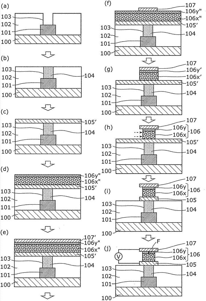
[0079] First, like figure 1 As shown in (a), a conductive layer made of aluminum or the like (with a film thickness of, for example, 400 nm or more and 600 nm or less) is formed on a substrate 100 on which transistors, lower wiring, etc. are formed, and patterned to form the lower wiring 101.

[0080] Then, after covering the lower layer wiring 101 and forming an insulating film on the substrate 100, the surface of the insulating film is planarized to form an interlayer insulating layer 102 (the film thickness is, for example, 500 nm or more and 1000 nm or less). Regarding the interlayer insulating layer 102, a plasma TEOS (Tetraethyl orthosilicate) film is used, or a fluorine-containing oxide (for example, FSG (Fluorinated Silicate Glass)) and other low-k materials are used to reduce the parasitic capacitance between wirings.

[0081] Then, the interlayer insulating layer 102 is patterned using a desired mask to form a contact hole 103 (a hole diameter of 50 nm or more and 300 nm o...

Embodiment approach 2

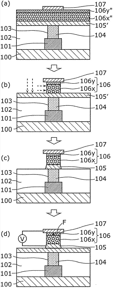
[0117] figure 2 (A) to (d) are cross-sectional views showing the method of manufacturing the main part of the nonvolatile memory element in the second embodiment of the present invention. in figure 2 (A) ~ (d), right and figure 1 (A) to (j) The same components are assigned the same symbols, and descriptions are omitted.

[0118] Such as figure 2 As shown in (a) to (d), the manufacturing method of the nonvolatile memory element of the first embodiment of the present invention is different from the manufacturing method of the nonvolatile memory element of the second embodiment of the present invention in that it differs from figure 1 The process of patterning the variable resistance film 106x" and the second variable resistance film 107y" shown in (g) and (h) simultaneously removes the side portion of the variable resistance element.

[0119] In the method of manufacturing the nonvolatile memory element of the first embodiment of the present invention, the variable resistance film ...

Embodiment approach 3

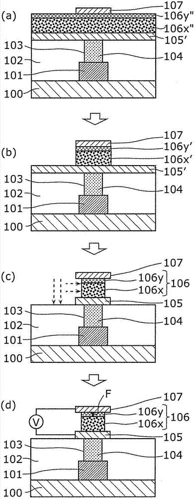
[0131] image 3 (A) to (d) are cross-sectional views showing the method of manufacturing the main part of the nonvolatile memory element in the third embodiment of the present invention. in image 3 (A) ~ (d), right and figure 1 (A) to (j) The same components are assigned the same reference numerals, and the description is omitted.

[0132] Such as image 3 As shown in (a) to (d), the difference between the manufacturing method of the non-volatile memory element of the first embodiment of the present invention and the method of manufacturing the non-volatile memory element of the third embodiment of the present invention is that they are performed simultaneously figure 1 Steps of removing the side portions of the variable resistance film 106x" and the second variable resistance film 107y" shown in (h) and (i) and patterning the first conductive film 105'.

[0133] In the manufacturing method of the nonvolatile memory element of the first embodiment of the present invention, after pa...


PUM

PropertyMeasurementUnit
Film thicknessaaaaaaaaaa

Abstract

This invention includes: a step (c) for forming a first electroconductive film (105') on a substrate; steps (d, e) for forming a first metal oxide layer (106x '), a second metal oxide layer (106y ') having a different level of oxygen deficiency to that of the first metal oxide layer, and a second electroconductive film (107'), on the first electroconductive film (105'); a step (f) for patterning the second electroconductive film (107') and thereby forming a second electrode (107); a step (g) for patterning the first metal oxide layer (106x ') and the second metal oxide layer (106y '), and thereby forming a variable resistance layer (106); a step (h) for removing the side section of the variable resistance layer (106) to a position further inward relative to the outline of the second electrode (107) on a plane parallel to the principal surface of the substrate; and a step (i) for patterning the first electroconductive film (105') and thereby forming a first electrode (105) after, or in the same step as, the step for removing the side section of the variable resistance layer (106).

Description

Technical field [0001] The present invention relates to a method for manufacturing a variable resistance nonvolatile memory element, and a nonvolatile memory element having a variable resistance element whose resistance value changes by application of an electric pulse. Background technique [0002] In recent years, with the advancement of digital technology, the functions of electronic devices such as portable information equipment and information appliances have further improved. With the increase in functionality of these electronic devices, the miniaturization and speeding of semiconductor elements used are rapidly progressing. Among them, the use of large-capacity nonvolatile memory represented by flash memory is rapidly expanding. Furthermore, as a next-generation new non-volatile memory that replaces this flash memory, research and development of a resistance variable memory (ReRAM: Resistive Random Access Memory) using variable resistance elements is being carried out. ...

Claims


Application Information

Patent Timeline
IPC IPC(8): H01L27/105H01L45/00H01L49/00
CPCH01L45/08H01L45/1675H01L45/16H01L49/00H01L45/146H01L45/1233H01L45/00H10N70/24H10N70/826H10N70/8833H10N70/063H10N70/011
Inventor 村濑英昭三河巧川岛良男姫野敦史
Owner PANASONIC CORP
Learn More