
Lens unit and laser processing device

A lens unit and laser processing technology, applied in auxiliary devices, measuring devices, metal processing, etc., can solve problems such as the inability to achieve the processing position accuracy per μm, and achieve the effect of high-precision laser processing

Active Publication Date: 2013-06-05
MITSUBISHI ELECTRIC CORP
View PDF8 Cites 9 Cited by
  • Summary
  • Abstract
  • Description
  • Claims
  • Application Information

AI Technical Summary

Problems solved by technology

In the laser processing equipment used in the processing of such high-definition electronic circuits and electronic components, the processing position accuracy in the unit of μm cannot be achieved by conventional laser markers and the like.

Method used


Image

  • Lens unit and laser processing device
  • Lens unit and laser processing device
  • Lens unit and laser processing device

Examples


Embodiment approach 1

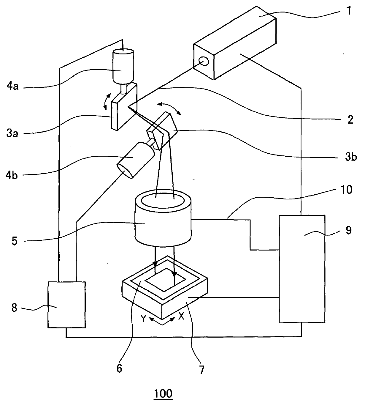
[0036] figure 1 It is an overall configuration diagram of the laser processing apparatus according to Embodiment 1 of the present invention.

[0037] Such as figure 1 As shown, the laser processing apparatus 100 of this embodiment includes a laser oscillator 1, a first galvano mirror 3a, a second galvano mirror 3b, a first galvano scanner 4a, a second galvano scanner 4b, and an fθ lens composed of a lens unit. 5. XY platform 7 , current driver 8 , and control device 9 .

[0038] The first galvano mirror 3a deflects the laser beam 2 output in the horizontal direction from the laser oscillator 1 in the horizontal plane.

[0039] The second galvano mirror 3b further deflects the laser beam 2 deflected by the 1st galvano mirror 3a in the vertical plane.

[0040] The first current scanner 4a drives the first current mirror 3a, and the second current scanner 4b drives the second current mirror 3b.

[0041] The fθ lens 5 is incident with the laser beam 2 deflected by the second g...

Embodiment approach 2

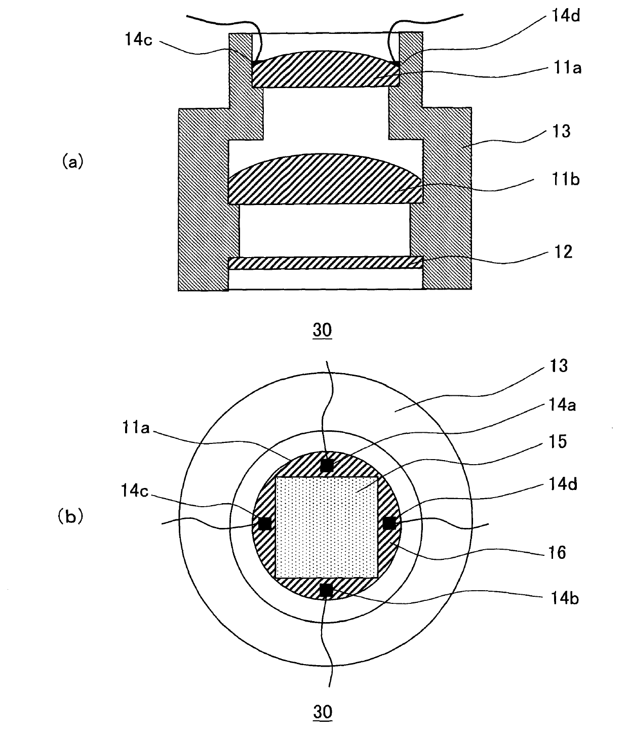
[0092] image 3 (a) is a schematic side sectional view of a lens unit used in the fθ lens of the laser processing apparatus according to Embodiment 2 of the present invention, image 3 (b) is a schematic top view of the lens unit on the incident side of the laser beam (b).

[0093] Such as image 3 As shown, the lens unit 30 used in the fθ lens of this embodiment is the same as the lens unit 20 of the first embodiment except that four temperature detectors are provided on the surface of the first optical lens 11a on the side where the laser beam 2 is incident. .

[0094] and, if image 3 As shown in (b), first, second, third, and fourth temperature detectors 14a, 14b, 14c, 14d.

[0095] In the case of using the lens unit 30 of the present embodiment as an fθ lens, as image 3 As shown in (b), four laser beam non-irradiation portions 16 that exist between the square or rectangular laser beam irradiation area 15 of the first optical lens 11a and the circular outer peripher...

Embodiment approach 3

[0135] Figure 4 (a) is a schematic side sectional view of a lens unit used in the fθ lens of the laser processing apparatus according to Embodiment 3 of the present invention, Figure 4(b) is a schematic diagram of the AA cross section of the lens unit in the schematic side cross-sectional diagram.

[0136] Such as Figure 4 As shown, the lens unit 40 used in the fθ lens of this embodiment is the same as the lens unit 20 of the first embodiment except that two temperature detectors 14 are provided on the surface of the second optical lens 11b on the side where the laser beam 2 is incident. .

[0137] Additionally, if Figure 4 As shown in (b), a temperature detector 14 is provided at each of both ends of a chord passing through the center point of the second optical lens 11b.

[0138] In the case of using the lens unit 40 of the present embodiment as an fθ lens, as Figure 4 As shown in (b), the area on the surface of the second optical lens 11b to which the laser beam 2...


PUM


Abstract

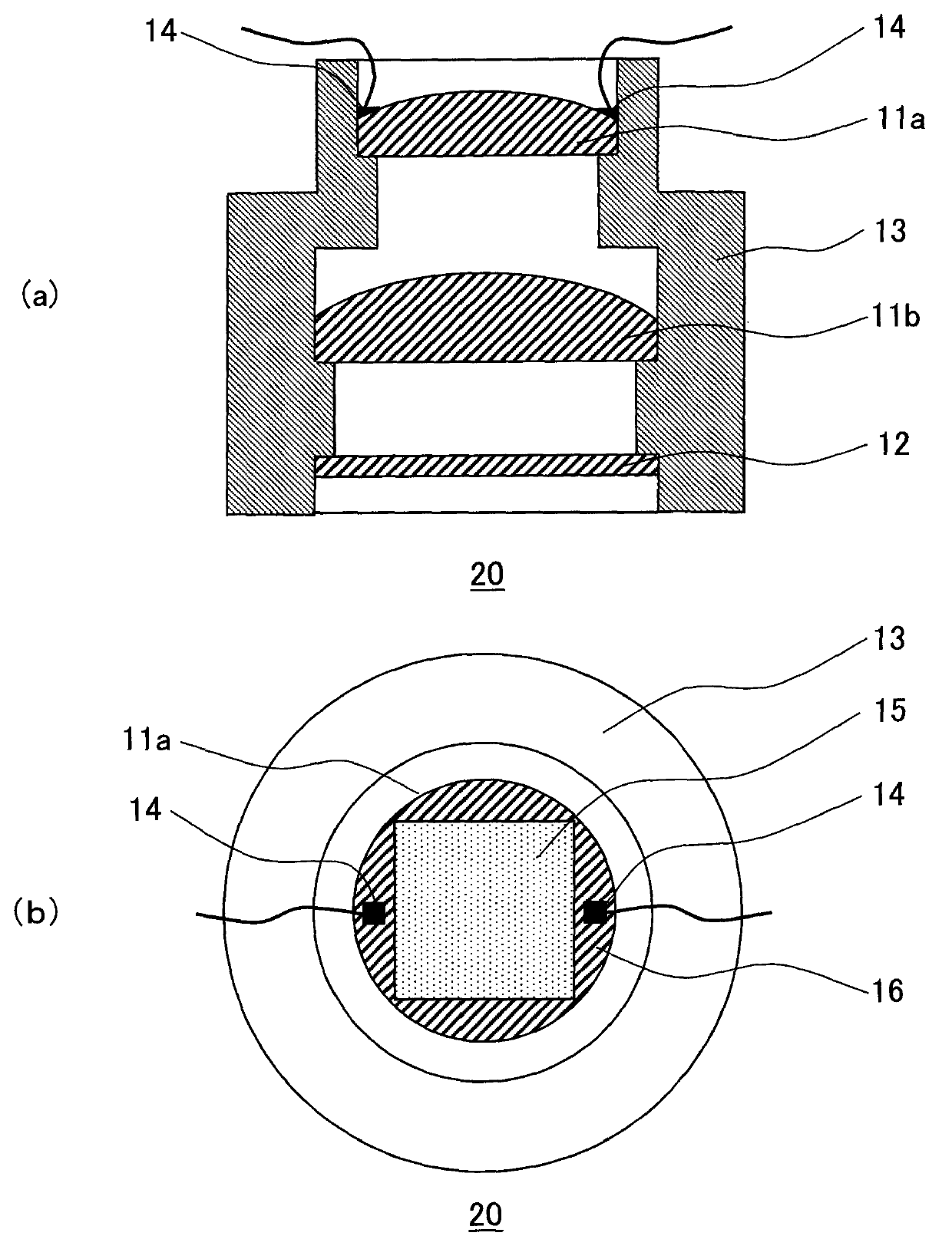
The invention provides a lens unit and a laser processing device. In the laser processing device (100), the lens unit (20) capable of measuring temperature change of optical lenses (11a, 11b) resulted from instant absorption of high-energy laser beams (2) by using temperature detectors (14) is used in a f[theta] lens. A plurality of temperature detectors (14) are disposed in non-irradiation part of the laser beams of the optical lenses (11a, 11b). A control device (9) corrects converged spot positions of the laser beams (2) according to temperature signals measured by the temperature detectors (14) to perform control.

Description

technical field [0001] The present invention relates to a lens unit for condensing and irradiating a laser beam perpendicularly to an object to be processed, and a laser processing device using the lens unit. Background technique [0002] A laser processing device using a galvano scanner has been used in laser engraving machines, laser marking machines, etc. in the past, and is generally known as a laser marker (laser marker). [0003] Recently, this laser processing device has been used in the process of drilling holes in multilayer printed circuit boards, precision electronic components, etc., as a precise, high-speed, and flexible processing method that replaces conventional drilling methods. [0004] In recent years, along with the miniaturization of semiconductors and the improvement of the degree of integration, the high-definition of electronic circuits and electronic components has become remarkable. In laser processing apparatuses used for processing such high-defi...

Claims


Application Information

Patent Timeline
Patent Type & Authority Applications(China)
IPC IPC(8): B23K26/00B23K26/06G02B7/02B23K26/04G01K1/14
CPCB23K26/046B23K26/0622B23K26/0643B23K26/0648B23K26/0853B23K37/0408B23K2101/42G03B30/00
Inventor 石塚智彦伊藤健治成濑正史高桥悌史
Owner MITSUBISHI ELECTRIC CORP
Learn More